- 您現(xiàn)在的位置:買賣IC網(wǎng) > PDF目錄361076 > NBC12429 (ON SEMICONDUCTOR) 3.3V/5V Programmable PLL Synthesized Clock Generator(3.3V/5V可編程PLL合成時(shí)鐘發(fā)生器) PDF資料下載
參數(shù)資料
| 型號(hào): | NBC12429 |
| 廠商: | ON SEMICONDUCTOR |
| 英文描述: | 3.3V/5V Programmable PLL Synthesized Clock Generator(3.3V/5V可編程PLL合成時(shí)鐘發(fā)生器) |
| 中文描述: | 3.3V/5V的可編程鎖相環(huán)路合成時(shí)鐘發(fā)生器(3.3V/5V的可編程PLL頻率合成時(shí)鐘發(fā)生器) |
| 文件頁(yè)數(shù): | 9/20頁(yè) |
| 文件大小: | 351K |
| 代理商: | NBC12429 |
第1頁(yè)第2頁(yè)第3頁(yè)第4頁(yè)第5頁(yè)第6頁(yè)第7頁(yè)第8頁(yè)當(dāng)前第9頁(yè)第10頁(yè)第11頁(yè)第12頁(yè)第13頁(yè)第14頁(yè)第15頁(yè)第16頁(yè)第17頁(yè)第18頁(yè)第19頁(yè)第20頁(yè)
NBC12429, NBC12429A
http://onsemi.com
9
PROGRAMMING INTERFACE
Programming the NBC12429 and NBC12429A is
accomplished by properly configuring the internal dividers
to produce the desired frequency at the outputs. The output
frequency can by represented by this formula:
FOUT
=
(FXTAL
÷
16)
×
M
÷
N
where F
XTAL
is the crystal frequency, M is the loop divider
modulus, and N is the output divider modulus. Note that it
is possible to select values of M such that thePLL isunable
toachievelooplock.Toavoidthis,alwaysmakesurethatM
isselectedtobe200
≤
M
≤
400fora16MHzinputreference.
Assuming that a 16 MHz reference frequency is used the
above equation reduces to:
FOUT
=
M
÷
N
Substituting the four values for N (1, 2, 4, 8) yields:
(eq. 1)
(eq. 2)
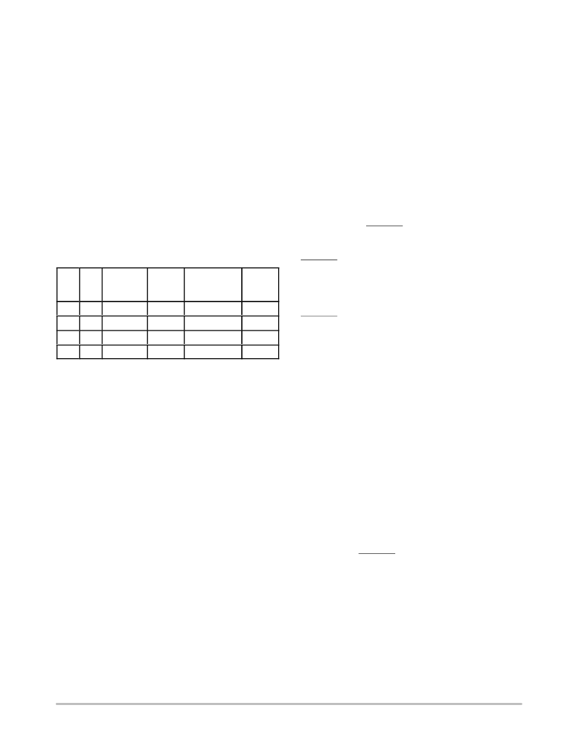
Table 10. Programmable Output Divider Function
N1
N0
N Divider
F
OUT
Output
Frequency
Range (MHz)*
F
OUT
Step
0
0
÷
1
÷
2
÷
4
÷
8
M
200--400
1 MHz
0
1
M
÷
2
M
÷
4
M
÷
8
100--200
500 kHz
1
0
50--100
250 kHz
1
1
25--50
125 kHz
*For crystal frequency of 16 MHz.
The user can identify the proper M and N values for the
desiredfrequencyfromtheaboveequations.Thefouroutput
frequency
ranges
established
200 MHz -- 400 MHz,
50 MHz -- 100 MHz and 25 MHz -- 50 MHz, respectively.
From these ranges, the user will establish the value of N
required. The value of M can then be calculated based on
Equation 1. For example, if an output frequency of
131 MHzwasdesired,thefollowingstepswouldbetakento
identify the appropriate M and N values. 131 MHz falls
within the frequency range set by an N value of 2; thus, N
[1:0] = 01. For N = 2, F
OUT
= M
÷
2 and M = 2 x F
OUT
.
Therefore,
M
=
131
×
2
=
262,soM[8 : 0]
=
100000110.
Following this same procedure, a user can generate any
whole frequency desired between 25 and 400 MHz. Note
thatforN>2,fractionalvaluesofF
OUT
canberealized.The
size of the programmable frequency steps (and thus, the
indicator of the fractional output frequencies achievable)
will be equal to F
XTAL
÷
16
÷
N.
For input reference frequencies other than 16 MHz, see
Table 11, which shows the usable VCO frequency and
M divider range.
by
N
are
100 MHz -- 200 MHz,
The input frequency and the selection of the feedback
divider M is limited by the VCO frequency range and
F
XTAL
. M must be configured to match the VCOfrequency
range of 200 MHz to 400 MHz in order to achieve stable
PLL operation.
Mmin
=
fVCOmin
÷
(fXTAL
÷
16) and
Mmax
=
fVCOmax
÷
(fXTAL
÷
16)
The value for M falls within the constraints set for PLL
stability. If the value for M fell outside of the valid range, a
different N value would be selected to move M in the
appropriate direction.
The M and N counters can be loaded either through a
parallel or serial interface. The parallel interface is
controlledviatheP_LOADsignalsuchthataLOWtoHIGH
transition will latch the information present on the M[8:0]
and N[1:0] inputs into the M and N counters. When the
P_LOAD signal is LOW, the input latches will be
transparentandanychangesontheM[8:0]andN[1:0]inputs
will affect the F
OUT
output pair. To use the serial port, the
S_CLOCK signal samples the information on the S_DATA
line and loads it into a 14 bit shift register. Note that the
P_LOADsignalmustbeHIGHfortheserialloadoperation
to function. The Test register is loaded with the first three
bits,theNregisterwiththenexttwo,andtheMregisterwith
the final nine bits of the data stream on the S_DATA input.
Foreachregister,themostsignificantbitisloadedfirst(T2,
N1, and M8). A pulse on the S_LOAD pin after the shift
registerisfullyloadedwilltransferthedividevaluesintothe
counters. The HIGH to LOW transition on the S_LOAD
input will latch the new divide values into the counters.
Figures 5 and 6 illustrate the timing diagram for both a
parallel and a serial load of the device synthesizer.
M[8:0] and N[1:0] are normally specified once at
powerup through the parallel interface, and then possibly
again through the serial interface. This approach allows the
application to comeupatonefrequency andthen changeor
fine--tune the clock as the ability to control the serial
interface becomes available.
TheTESToutputprovidesvisibilityforoneoftheseveral
internal nodes as determined by the T[2:0] bits in the serial
configuration stream. It is not configurable through the
parallelinterface.TheT2,T1,andT0controlbitsarepreset
to ‘000’ when P_LOAD is LOW so that the PECL F
OUT
outputsareasjitter--freeaspossible.Anyactivesignalonthe
TEST output pin will have detrimental affects on the jitter
of the PECL output pair. In normal operations, jitter
specifications are only guaranteed if the TEST output is
static.Theserialconfigurationportcanbeusedtoselectone
of the alternate functions for this pin.
(eq. 3)
(eq. 4)
相關(guān)PDF資料 |
PDF描述 |
|---|---|
| NBC12429A | 3.3V/5V Programmable PLL Synthesized Clock Generator(3.3V/5V可編程PLL合成時(shí)鐘發(fā)生器) |
| NBC12430 | 3.3V/5V Programmable PLL Synthesized Clock Generator(3.3V/5V可編程PLL合成時(shí)鐘發(fā)生器) |
| NBC12430A | 3.3V/5V Programmable PLL Synthesized Clock Generator(3.3V/5V可編程PLL合成時(shí)鐘發(fā)生器) |
| NBC12439A | 3.3V/5V Programmable PLL Synthesized Clock Generator(3.3V/5V可編程PLL合成時(shí)鐘發(fā)生器) |
| NBC12439 | 3.3V/5V Programmable PLL Synthesized Clock Generator(3.3V/5V可編程PLL合成時(shí)鐘發(fā)生器) |
相關(guān)代理商/技術(shù)參數(shù) |
參數(shù)描述 |
|---|---|
| NBC12429/D | 制造商:ONSEMI 制造商全稱:ON Semiconductor 功能描述:3.3 V/5 V Programmable PLL Synthesized Clock Generator (25 to 400 MHz) |
| NBC12429_07 | 制造商:ONSEMI 制造商全稱:ON Semiconductor 功能描述:3.3V/5V Programmable PLL Synthesized Clock Generator |
| NBC12429A | 制造商:ONSEMI 制造商全稱:ON Semiconductor 功能描述:3.3V/5V Programmable PLL Synthesized Clock Generator |
| NBC12429AFA | 功能描述:鎖相環(huán) - PLL 3.3V/5V Programmable RoHS:否 制造商:Silicon Labs 類型:PLL Clock Multiplier 電路數(shù)量:1 最大輸入頻率:710 MHz 最小輸入頻率:0.002 MHz 輸出頻率范圍:0.002 MHz to 808 MHz 電源電壓-最大:3.63 V 電源電壓-最小:1.71 V 最大工作溫度:+ 85 C 最小工作溫度:- 40 C 封裝 / 箱體:QFN-36 封裝:Tray |
| NBC12429AFAG | 功能描述:鎖相環(huán) - PLL 3.3V/5V Programmable PLL Clock Generator RoHS:否 制造商:Silicon Labs 類型:PLL Clock Multiplier 電路數(shù)量:1 最大輸入頻率:710 MHz 最小輸入頻率:0.002 MHz 輸出頻率范圍:0.002 MHz to 808 MHz 電源電壓-最大:3.63 V 電源電壓-最小:1.71 V 最大工作溫度:+ 85 C 最小工作溫度:- 40 C 封裝 / 箱體:QFN-36 封裝:Tray |
發(fā)布緊急采購(gòu),3分鐘左右您將得到回復(fù)。