- 您現(xiàn)在的位置:買賣IC網(wǎng) > PDF目錄224594 > N74F109D-T (NXP SEMICONDUCTORS) Positive J-Knot positive edge-triggered flip-flops - Description: Dual J-/K Flip-Flop with Set and Reset; Positive-Edge Trigger ; F<sub>max</sub>: 125 MHz; Logic switching levels: TTL ; Number of pins: 14 ; Output drive capability: -1/+20 mA ; Propagation delay: 6.2 ns; Voltage: 4.5-5.5 V PDF資料下載
參數(shù)資料
| 型號(hào): | N74F109D-T |
| 廠商: | NXP SEMICONDUCTORS |
| 元件分類: | 鎖存器 |
| 英文描述: | Positive J-Knot positive edge-triggered flip-flops - Description: Dual J-/K Flip-Flop with Set and Reset; Positive-Edge Trigger ; F<sub>max</sub>: 125 MHz; Logic switching levels: TTL ; Number of pins: 14 ; Output drive capability: -1/+20 mA ; Propagation delay: 6.2 ns; Voltage: 4.5-5.5 V |
| 中文描述: | F/FAST SERIES, DUAL POSITIVE EDGE TRIGGERED J-KBAR FLIP-FLOP, COMPLEMENTARY OUTPUT, PDSO16 |
| 封裝: | 3.9 MM, PLASTIC, SOT109-1, SO-16 |
| 文件頁(yè)數(shù): | 4/10頁(yè) |
| 文件大小: | 95K |
| 代理商: | N74F109D-T |
Philips Semiconductors
Product specification
74F109
Postive J-K positive edge-triggered flip-flops
October 23, 1990
3
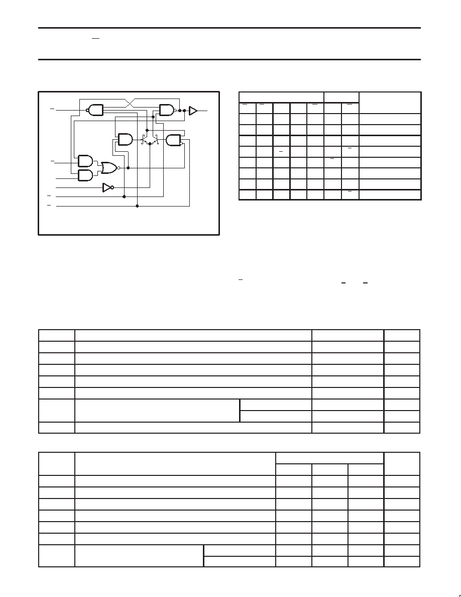
LOGIC DIAGRAM
VCC = Pin 16
GND = Pin 8
K
Q
CP
4, 12
3, 13
6, 10
7, 9
2, 14
5, 11
1, 15
SD
RD
J
SF00138
FUNCTION TABLE
INPUTS
OUTPUTS
OPERATING MODE
SD
RD
CP
J
K
Q
OPERATING MODE
L
H
X
H
L
Asynchronous set
H
L
X
L
H
Asynchronous reset
L
X
H
Undetermined*
H
↑
X
q
Hold
H
↑
h
l
q
Toggle
H
↑
h
H
L
Load ”1” (set)
H
↑
l
L
H
Load ”0” (reset)
H
↑
l
h
q
Hold ’no change”
NOTES:
H = High-voltage level
h
= High-voltage level one setup time prior to low-to-high
clock transition
L
= Low-voltage level
l
= Low-voltage level one setup time prior to low-to-high
clock transition
q
= Lower case indicate the state of the referenced output
prior to the low-to-high clock transition
X = Don’t care
↑ = Low-to-high clock transition
↑ = Not low-to-high clock transition
*
= Both outputs will be high if both SD and RD go low
simultaneously
ABSOLUTE MAXIMUM RATINGS
(Operation beyond the limit set forth in this table may impair the useful life of the device. Unless otherwise noted these limits are over the
operating free air temperature range.)
SYMBOL
PARAMETER
RATING
UNIT
VCC
Supply voltage
–0.5 to +7.0
V
VIN
Input voltage
–0.5 to +7.0
V
IIN
Input current
–30 to +5
mA
VOUT
Voltage applied to output in High output state
–0.5 to VCC
V
IOUT
Current applied to output in Low output state
40
mA
T
Operating free air temperature range
Commercial range
0 to +70
°C
Tamb
Operating free-air temperature range
Industrial range
–40 to +85
°C
Tstg
Storage temperature range
–65 to +150
°C
RECOMMENDED OPERATING CONDITIONS
SYMBOL
PARAMETER
LIMITS
UNIT
SYMBOL
PARAMETER
MIN
NOM
MAX
UNIT
VCC
Supply voltage
4.5
5.0
5.5
V
VIN
High-level input voltage
2.0
V
VIL
Low-level input voltage
0.8
V
IIK
Input clamp current
–18
mA
IOH
High-level output current
–1
mA
IOL
Low-level output current
20
mA
T
Operating free air temperature range
Commercial range
0
+70
°C
Tamb
Operating free-air temperature range
Industrial range
–40
+85
°C
相關(guān)PDF資料 |
PDF描述 |
|---|---|
| N74F1244D-T | Octal buffer (3-State) - Description: Buffer/Light Load F244 (3-State) ; Logic switching levels: TTL ; Number of pins: 20 ; Output drive capability: -15/+64 mA ; Propagation delay: 5 ns; Voltage: 4.5-5.5 V |
| N74F125D-T | Quad buffers (3-State) - Description: Quad Buffer/Line Driver with Active LOW Output Enable (3-State) ; Logic switching levels: TTL ; Number of pins: 14 ; Output drive capability: -15/+64 mA ; Propagation delay: 5 ns; Voltage: 4.5-5.5 V |
| N74F126D-T | Quad buffers (3-State) - Description: Quad Buffer/Line Driver with Active HIGH Output Enable (3-State) ; Logic switching levels: TTL ; Number of pins: 14 ; Output drive capability: -15/+64 mA ; Propagation delay: 5 ns; Voltage: 4.5-5.5 V |
| N74F138D-T | 1-of-8 decoder/demultiplexer - Description: 3-to-8 Line Decoder/Demultiplexer; Inverting ; Logic switching levels: TTL ; Number of pins: 16 ; Output drive capability: -1/+20 mA ; Propagation delay: 6.1 ns; Voltage: 4.5-5.5 V |
| N74F139D-T | Dual 1-of-4 decoder/demultiplexer - Description: Dual 2-to-4 Line Decoder/Demultiplexer ; Logic switching levels: TTL ; Number of pins: 16 ; Output drive capability: -1/+20 mA ; Propagation delay: 5.3 ns; Voltage: 4.5-5.5 V |
相關(guān)代理商/技術(shù)參數(shù) |
參數(shù)描述 |
|---|---|
| N74F109N | 功能描述:觸發(fā)器 DUAL J-K POS EDGE RoHS:否 制造商:Texas Instruments 電路數(shù)量:2 邏輯系列:SN74 邏輯類型:D-Type Flip-Flop 極性:Inverting, Non-Inverting 輸入類型:CMOS 輸出類型: 傳播延遲時(shí)間:4.4 ns 高電平輸出電流:- 16 mA 低電平輸出電流:16 mA 電源電壓-最大:5.5 V 最大工作溫度:+ 85 C 安裝風(fēng)格:SMD/SMT 封裝 / 箱體:X2SON-8 封裝:Reel |
| N74F109N,602 | 功能描述:觸發(fā)器 DUAL J-K POS EDGE RoHS:否 制造商:Texas Instruments 電路數(shù)量:2 邏輯系列:SN74 邏輯類型:D-Type Flip-Flop 極性:Inverting, Non-Inverting 輸入類型:CMOS 輸出類型: 傳播延遲時(shí)間:4.4 ns 高電平輸出電流:- 16 mA 低電平輸出電流:16 mA 電源電壓-最大:5.5 V 最大工作溫度:+ 85 C 安裝風(fēng)格:SMD/SMT 封裝 / 箱體:X2SON-8 封裝:Reel |
| N74F10D | 功能描述:邏輯門(mén) TRIPLE 3-INPUT NAND GATE RoHS:否 制造商:Texas Instruments 產(chǎn)品:OR 邏輯系列:LVC 柵極數(shù)量:2 線路數(shù)量(輸入/輸出):2 / 1 高電平輸出電流:- 16 mA 低電平輸出電流:16 mA 傳播延遲時(shí)間:3.8 ns 電源電壓-最大:5.5 V 電源電壓-最小:1.65 V 最大工作溫度:+ 125 C 安裝風(fēng)格:SMD/SMT 封裝 / 箱體:DCU-8 封裝:Reel |
| N74F10D,602 | 功能描述:邏輯門(mén) TRIPLE 3-INPUT NAND RoHS:否 制造商:Texas Instruments 產(chǎn)品:OR 邏輯系列:LVC 柵極數(shù)量:2 線路數(shù)量(輸入/輸出):2 / 1 高電平輸出電流:- 16 mA 低電平輸出電流:16 mA 傳播延遲時(shí)間:3.8 ns 電源電壓-最大:5.5 V 電源電壓-最小:1.65 V 最大工作溫度:+ 125 C 安裝風(fēng)格:SMD/SMT 封裝 / 箱體:DCU-8 封裝:Reel |
| N74F10D,623 | 功能描述:邏輯門(mén) TRIPLE 3-INPUT NAND RoHS:否 制造商:Texas Instruments 產(chǎn)品:OR 邏輯系列:LVC 柵極數(shù)量:2 線路數(shù)量(輸入/輸出):2 / 1 高電平輸出電流:- 16 mA 低電平輸出電流:16 mA 傳播延遲時(shí)間:3.8 ns 電源電壓-最大:5.5 V 電源電壓-最小:1.65 V 最大工作溫度:+ 125 C 安裝風(fēng)格:SMD/SMT 封裝 / 箱體:DCU-8 封裝:Reel |
發(fā)布緊急采購(gòu),3分鐘左右您將得到回復(fù)。