- 您現(xiàn)在的位置:買(mǎi)賣(mài)IC網(wǎng) > PDF目錄383644 > MT9040 (Mitel Networks Corporation) T1/E1 Synchronizer(T1/E1 系統(tǒng)同步裝置(由一個(gè)數(shù)字鎖相環(huán)組成)) PDF資料下載
參數(shù)資料
| 型號(hào): | MT9040 |
| 廠商: | Mitel Networks Corporation |
| 英文描述: | T1/E1 Synchronizer(T1/E1 系統(tǒng)同步裝置(由一個(gè)數(shù)字鎖相環(huán)組成)) |
| 中文描述: | 的T1/E1同步(T1/E1的系統(tǒng)同步裝置(由一個(gè)數(shù)字鎖相環(huán)組成)) |
| 文件頁(yè)數(shù): | 4/20頁(yè) |
| 文件大小: | 82K |
| 代理商: | MT9040 |
第1頁(yè)第2頁(yè)第3頁(yè)當(dāng)前第4頁(yè)第5頁(yè)第6頁(yè)第7頁(yè)第8頁(yè)第9頁(yè)第10頁(yè)第11頁(yè)第12頁(yè)第13頁(yè)第14頁(yè)第15頁(yè)第16頁(yè)第17頁(yè)第18頁(yè)第19頁(yè)第20頁(yè)
MT9040
Advance Information
4
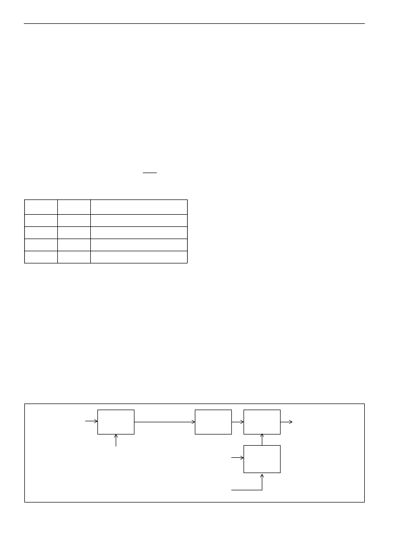
Figure 3 - DPLL Block Diagram
Control
Circuit
State Select
from
Input Impairment Monitor
State Select
from
State Machine
Feedback Signal
from
Frequency Select MUX
DPLL Reference
to
Output Interface Circuit
Loop Filter
Digitally
Controlled
Oscillator
Phase
Detector
Reference
Functional Description
The
providing timing (clock) and synchronization (frame)
signals to interface circuits for T1 and E1 Primary
Rate Digital Transmission links. Figure 1 is a
functional block diagram which is described in the
following sections.
MT9040
is
a
T1/E1
Trunk
Synchronizer,
Frequency Select MUX Circuit
The MT9040 operates on the falling edge of the
reference. It operates with one of four possible input
reference frequencies (8kHz, 1.544MHz, 2.048MHz
or 19.44MHz). The frequency select inputs (FS1 and
FS2) determine which of the four frequencies may be
used at the reference input. A reset (RST) must be
performed after every frequency select input change.
See Table 1.
Table 1 - Input Frequency Selection
Digital Phase Lock Loop (DPLL)
As shown in Figure 3, the DPLL of the MT9040
consists of a Phase Detector, Loop Filter, Digitally
Controlled Oscillator and a Control Circuit.
Phase Detector
- the Phase Detector compares the
reference signal with the feedback signal from the
Frequency Select MUX circuit, and provides an error
signal
corresponding
to
between the two. This error signal is passed to the
Loop Filter. The Frequency Select MUX allows the
proper feedback signal to be externally selected
(e.g., 8kHz, 1.544MHz, 2.048MHz or 19.44MHz).
the
phase
difference
Loop Filter
- the Loop Filter is similar to a first order
low pass filter with a 1.9 Hz cutoff frequency for all
four
reference
frequency
1.544MHz, 2.048MHz or 19.44MHz). This filter
ensures that the network jitter transfer requirements
are met.
selections
(8kHz,
Control Circuit
- the Control Circuit uses status and
control information from the State Machine and the
Input Impairment Circuit to set the mode of the
DPLL. The two possible modes are Normal and
Freerun.
Digitally Controlled Oscillator (DCO)
- the DCO
receives the filtered signal from the Loop Filter, and
based on its value, generates a corresponding digital
output signal. The synchronization method of the
DCO is dependent on the state of the MT9040.
In Normal Mode, the DCO provides an output signal
which is frequency and phase locked to the input
reference signal.
In Freerun Mode, the DCO is free running with an
accuracy equal to the accuracy of the OSCi 20MHz
source.
Lock Indicator
- If the PLL is in frequency lock
(frequency lock means the center frequency of the
PLL is identical to the line frequency), and the input
phase offset is small, then the lock signal will be set
high.
Output Interface Circuit
The output of the DCO (DPLL) is used by the Output
Interface Circuit to provide the output signals shown
in Figure 4. The Output Interface Circuit uses four
Tapped Delay Lines followed by a T1 Divider Circuit,
an E1 Divider Circuit, and a DS2 Divider Circuit to
generate the required output signals.
FS2
FS1
Input Frequency
0
0
19.44MHz
0
1
8kHz
1
0
1.544MHz
1
1
2.048MHz
相關(guān)PDF資料 |
PDF描述 |
|---|---|
| MT9041A | () |
| MT9041B | T1/E1 System Synchronizer(T1/E1系統(tǒng)同步裝置(由一個(gè)數(shù)字鎖相環(huán)組成)) |
| MT9042B | () |
| MT9042C | Multitrunk System Synchronizer(多中繼系統(tǒng)同步裝置) |
| MT9043 | T1/E1 System Synchronizer(T1/E1 系統(tǒng)同步裝置(由一個(gè)數(shù)字鎖相環(huán)組成)) |
相關(guān)代理商/技術(shù)參數(shù) |
參數(shù)描述 |
|---|---|
| MT90401 | 制造商:ZARLINK 制造商全稱(chēng):Zarlink Semiconductor Inc 功能描述:SONET/SDH Clock Multiplier PLL |
| MT90401AB | 制造商:ZARLINK 制造商全稱(chēng):Zarlink Semiconductor Inc 功能描述:SONET/SDH System Synchronizer |
| MT90401AB1 | 制造商:Microsemi Corporation 功能描述:FRAMER SDH/SONET 3.3V 80LQFP EP - Trays 制造商:MICROSEMI CONSUMER MEDICAL PRODUCT GROUP 功能描述:IC SYNCHRONIZER SONET/SDH 80LQFP 制造商:Microsemi Corporation 功能描述:IC SYNCHRONIZER SONET/SDH 80LQFP |
| MT9040AN | 制造商:ZARLINK 制造商全稱(chēng):Zarlink Semiconductor Inc 功能描述:T1/E1 Synchronizer |
| MT9040AN1 | 制造商:Microsemi Corporation 功能描述:FRAMER E1 /T1 3.3V 48SSOP - Rail/Tube |
發(fā)布緊急采購(gòu),3分鐘左右您將得到回復(fù)。