- 您現(xiàn)在的位置:買賣IC網(wǎng) > PDF目錄384759 > MT90221 (Mitel Networks Corporation) Quad IMA/UNI PHY Device PDF資料下載
參數(shù)資料
| 型號(hào): | MT90221 |
| 廠商: | Mitel Networks Corporation |
| 英文描述: | Quad IMA/UNI PHY Device |
| 中文描述: | 四IMA的/單向物理層設(shè)備 |
| 文件頁(yè)數(shù): | 90/114頁(yè) |
| 文件大小: | 304K |
| 代理商: | MT90221 |
第1頁(yè)第2頁(yè)第3頁(yè)第4頁(yè)第5頁(yè)第6頁(yè)第7頁(yè)第8頁(yè)第9頁(yè)第10頁(yè)第11頁(yè)第12頁(yè)第13頁(yè)第14頁(yè)第15頁(yè)第16頁(yè)第17頁(yè)第18頁(yè)第19頁(yè)第20頁(yè)第21頁(yè)第22頁(yè)第23頁(yè)第24頁(yè)第25頁(yè)第26頁(yè)第27頁(yè)第28頁(yè)第29頁(yè)第30頁(yè)第31頁(yè)第32頁(yè)第33頁(yè)第34頁(yè)第35頁(yè)第36頁(yè)第37頁(yè)第38頁(yè)第39頁(yè)第40頁(yè)第41頁(yè)第42頁(yè)第43頁(yè)第44頁(yè)第45頁(yè)第46頁(yè)第47頁(yè)第48頁(yè)第49頁(yè)第50頁(yè)第51頁(yè)第52頁(yè)第53頁(yè)第54頁(yè)第55頁(yè)第56頁(yè)第57頁(yè)第58頁(yè)第59頁(yè)第60頁(yè)第61頁(yè)第62頁(yè)第63頁(yè)第64頁(yè)第65頁(yè)第66頁(yè)第67頁(yè)第68頁(yè)第69頁(yè)第70頁(yè)第71頁(yè)第72頁(yè)第73頁(yè)第74頁(yè)第75頁(yè)第76頁(yè)第77頁(yè)第78頁(yè)第79頁(yè)第80頁(yè)第81頁(yè)第82頁(yè)第83頁(yè)第84頁(yè)第85頁(yè)第86頁(yè)第87頁(yè)第88頁(yè)第89頁(yè)當(dāng)前第90頁(yè)第91頁(yè)第92頁(yè)第93頁(yè)第94頁(yè)第95頁(yè)第96頁(yè)第97頁(yè)第98頁(yè)第99頁(yè)第100頁(yè)第101頁(yè)第102頁(yè)第103頁(yè)第104頁(yè)第105頁(yè)第106頁(yè)第107頁(yè)第108頁(yè)第109頁(yè)第110頁(yè)第111頁(yè)第112頁(yè)第113頁(yè)第114頁(yè)
MT90221
82
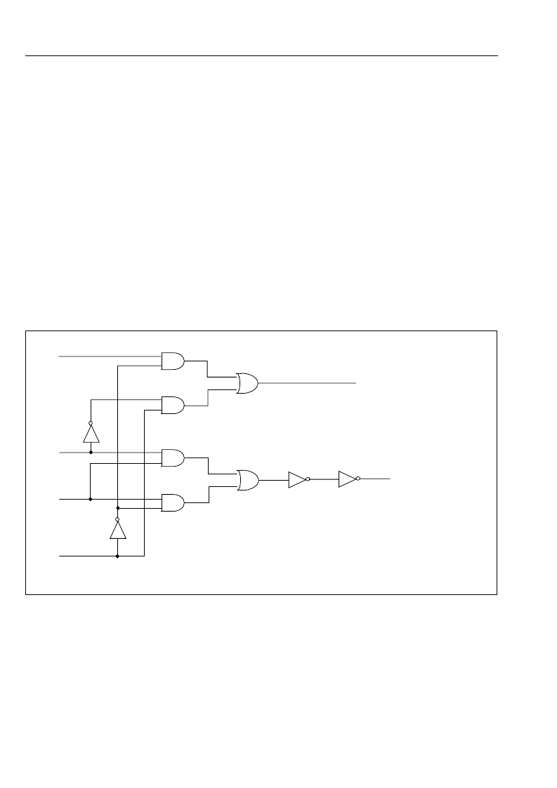
8.2
Optimum Usage of 1 Bank of Memory with
a 4 Port Device
Due to the addressing mode of the MT90221, only
half of the memory locations are utilized when
operating in IMA mode. This is mainly due to the fact
that only links 0 to 3 can be used. With some
external circuitry, the addressing can be altered to
gain access to the unused half of the memory that
would correspond to the links 4 to 7.
Figure 23 shows how this can be achieved. The CS0
and CS1 signals are merged to generate a unique
CS0. The address bit 8 is not modified when bank 0
is accessed and it is inverted when the bank 1 is
accessed. The CTRL signal is included to enable or
disable the re-mapping circuitry in the case where a
layout is including stuffing options for an 8 port or a 4
port implementation. If the control feature is not
required, the circuitry can be simplified.
Figure 23 -Memory Optimization for the MT90221
U5
U6
U9
U10
U1
U2
U3
U4
U8
U7
ADDRo_8
CSo_0
CTRL
CSi_0
CSi_1
ADDRi_8
CTRL = 0 -> Normal Operation
CTRL = 1 -> Single Bank Operation
Note:
The two inverters, U9 and U10 here are to
make up a small delay to ensure that
CSo_0 comes after ADDRo_8 when in Single
Bank mode (in this mode, CSi_1 is routed to
both CSo_0 and ADDRo_8)
相關(guān)PDF資料 |
PDF描述 |
|---|---|
| MT90221AL | Quad IMA/UNI PHY Device |
| MT9041B | T1/E1 System Synchronizer |
| MT9041BP | T1/E1 System Synchronizer |
| MT9041 | Multiple Output Trunk PLL |
| MT9041AP | IC REG LDO 150MA 5.0V 0.5% 8SOIC |
相關(guān)代理商/技術(shù)參數(shù) |
參數(shù)描述 |
|---|---|
| MT90221AL | 制造商:MITEL 制造商全稱:Mitel Networks Corporation 功能描述:Quad IMA/UNI PHY Device |
| MT90222 | 制造商:ZARLINK 制造商全稱:Zarlink Semiconductor Inc 功能描述:4/8/16 Port IMA/TC PHY Device |
| MT90222AG | 制造商:Microsemi Corporation 功能描述:ATM IMA 40MBPS 2.5V 384BGA - Trays |
| MT90222AG2 | 制造商:Microsemi Corporation 功能描述:ATM IMA 40MBPS 2.5V 384BGA /BAKE/DRYPACK - Trays |
| MT90223AG | 制造商:Microsemi Corporation 功能描述:ATM IMA 80MBPS 2.5V 384BGA - Trays |
發(fā)布緊急采購(gòu),3分鐘左右您將得到回復(fù)。