- 您現(xiàn)在的位置:買賣IC網(wǎng) > PDF目錄385639 > MT46V4M32LG (Micron Technology, Inc.) I.MX31 LITE KIT PDF資料下載
參數(shù)資料
| 型號: | MT46V4M32LG |
| 廠商: | Micron Technology, Inc. |
| 英文描述: | I.MX31 LITE KIT |
| 中文描述: | 雙倍數(shù)據(jù)速率的DDR SDRAM內存 |
| 文件頁數(shù): | 58/66頁 |
| 文件大?。?/td> | 1921K |
| 代理商: | MT46V4M32LG |
第1頁第2頁第3頁第4頁第5頁第6頁第7頁第8頁第9頁第10頁第11頁第12頁第13頁第14頁第15頁第16頁第17頁第18頁第19頁第20頁第21頁第22頁第23頁第24頁第25頁第26頁第27頁第28頁第29頁第30頁第31頁第32頁第33頁第34頁第35頁第36頁第37頁第38頁第39頁第40頁第41頁第42頁第43頁第44頁第45頁第46頁第47頁第48頁第49頁第50頁第51頁第52頁第53頁第54頁第55頁第56頁第57頁當前第58頁第59頁第60頁第61頁第62頁第63頁第64頁第65頁第66頁
58
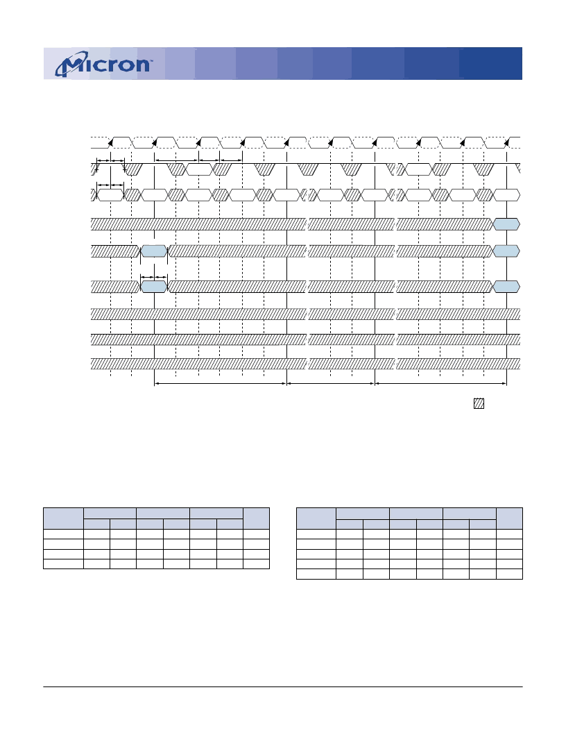
128Mb: x32 DDR SDRAM
4M32DDR_B.p65 – Rev. B, Pub. 7/02
Micron Technology, Inc., reserves the right to change products or specifications without notice.
2002, Micron Technology, Inc.
128Mb: x32
DDR SDRAM
ADVANCE
AUTO REFRESH MODE
CK
CK#
COMMAND
1
NOP
2
VALID
VALID
NOP
2
NOP
2
PRE
CKE
RA
A0-A7, A9-A11
A8
1
BA0, BA1
1
Bank(s)
3
BA
NOTE
:
1. PRE = PRECHARGE, ACT = ACTIVE, AR = AUTO REFRESH, RA = Row Address, BA = Bank Address.
2. NOP commands are shown for ease of illustration; other valid commands may be possible at these times.
3. Don t Care if A8 is HIGH at this point; A8 must be HIGH if more than one bank is active (i.e., must precharge all active banks).
4. DM, DQ and DQS signals are all Don t Care /High-Z for operations shown.
5. The second AUTO REFRESH is not required and is only shown as an example of two back-to-back AUTO REFRESH commands.
AR
NOP
2
AR
5
NOP2
ACT
NOP2
ONE BANK
ALL BANKS
t
CK
t
CH
t
CL
t
IS
t
IS
t
IH
t
IH
t
IS
t
IH
RA
(
)
(
)
(
)
(
)
(
)
(
)
(
)
(
)
(
)
(
)
(
)
(
)
(
)
(
)
(
)
(
)
(
)
(
)
(
)
(
)
(
)
(
)
(
)
(
)
(
)
(
)
(
)
(
)
(
)
(
)
(
)
(
)
(
)
(
)
(
)
(
)
(
)
(
)
(
)
(
)
(
)
(
)
(
)
(
)
(
)
(
)
(
)
(
)
DQ
4
DM
4
DQS
4
(
)
(
)
(
)
(
)
(
)
(
)
(
)
(
(
)
(
)
)
(
)
(
)
(
)
(
)
(
)
(
)
(
)
(
)
(
)
(
(
)
(
)
)
(
)
(
)
tRFC
5
tRP
tRFC
T0
T1
T2
T3
T4
Ta0
Tb0
Ta1
Tb1
Tb2
DON T CARE
TIMING PARAMETERS
-33
-4
-5
SYMBOL
t
CH
t
CL
t
CK (5)
t
CK (4)
MIN
0.45
0.45
3.3
4
MAX
0.55
0.55
8
8
MIN
0.45
0.45
-
4
MAX
0.55
0.55
-
8
MIN
0.45
0.45
-
-
MAX
0.55
0.55
-
-
UNITS
t
CK
t
CK
ns
ns
-33
-4
-5
SYMBOL
t
CK (3)
t
IH
t
IS
t
RFC
t
RP
MIN
-
0.9
0.9
62
16
MAX
-
MIN
-
0.9
0.9
62
16
MAX
-
MIN
5
0.9
0.9
62
20
MAX
8
UNITS
ns
ns
ns
ns
ns
相關PDF資料 |
PDF描述 |
|---|---|
| MT46V64M4 | 16 Meg x 4 x 4 banks DDR SDRAM(16M x 4 x 4組,雙數(shù)據(jù)速率同步動態(tài)RAM) |
| MT46V64M8 | 16 Meg x 8 x 4 banks DDR SDRAM(16M x 8 x 4組,雙數(shù)據(jù)速率同步動態(tài)RAM) |
| MT48LC16M8A1TG | SYNCHRONOUS DRAM |
| MT48LC32M4A1 | ECONOLINE: RSZ/P - 1kVDC |
| MT48LC32M4A2 | SYNCHRONOUS DRAM |
相關代理商/技術參數(shù) |
參數(shù)描述 |
|---|---|
| MT46V64M16 | 制造商:MICRON 制造商全稱:Micron Technology 功能描述:DOUBLE DATA RATE (DDR) SDRAM |
發(fā)布緊急采購,3分鐘左右您將得到回復。