- 您現(xiàn)在的位置:買賣IC網(wǎng) > PDF目錄385639 > MT46V4M32LG (Micron Technology, Inc.) I.MX31 LITE KIT PDF資料下載
參數(shù)資料
| 型號: | MT46V4M32LG |
| 廠商: | Micron Technology, Inc. |
| 英文描述: | I.MX31 LITE KIT |
| 中文描述: | 雙倍數(shù)據(jù)速率的DDR SDRAM內(nèi)存 |
| 文件頁數(shù): | 24/66頁 |
| 文件大?。?/td> | 1921K |
| 代理商: | MT46V4M32LG |
第1頁第2頁第3頁第4頁第5頁第6頁第7頁第8頁第9頁第10頁第11頁第12頁第13頁第14頁第15頁第16頁第17頁第18頁第19頁第20頁第21頁第22頁第23頁當(dāng)前第24頁第25頁第26頁第27頁第28頁第29頁第30頁第31頁第32頁第33頁第34頁第35頁第36頁第37頁第38頁第39頁第40頁第41頁第42頁第43頁第44頁第45頁第46頁第47頁第48頁第49頁第50頁第51頁第52頁第53頁第54頁第55頁第56頁第57頁第58頁第59頁第60頁第61頁第62頁第63頁第64頁第65頁第66頁
24
128Mb: x32 DDR SDRAM
4M32DDR_B.p65 – Rev. B, Pub. 7/02
Micron Technology, Inc., reserves the right to change products or specifications without notice.
2002, Micron Technology, Inc.
128Mb: x32
DDR SDRAM
ADVANCE
WRITEs
WRITE bursts are initiated with a WRITE command,
as shown in Figure 14.
The starting column and bank addresses are pro-
vided with the WRITE command, and auto precharge
is either enabled or disabled for that access. If auto
precharge is enabled, the row being accessed is
precharged at the completion of the burst. For the ge-
neric WRITE commands used in the following illustra-
tions, auto precharge is disabled.
During WRITE bursts, the first valid data-in ele-
ment will be registered on the first rising edge of DQS
following the WRITE command, and subsequent data
elements will be registered on successive edges of DQS.
The LOW state on DQS between the WRITE command
and the first rising edge is known as the write preamble;
the LOW state on DQS following the last data-in ele-
ment is known as the write postamble.
The time between the WRITE command and the
first corresponding rising edge of DQS (
t
DQSS) is speci-
fied with a relatively wide range (from 75 percent to 125
percent of one clock cycle). All of the WRITE diagrams
show the nominal case, and where the two extreme
cases (i.e.,
t
DQSS [MIN] and
t
DQSS
[MAX]) might not be
intuitive, they have also been included. Figure 15 shows
the nominal case and the extremes of
t
DQSS for a burst
of 4. Upon completion of a burst, assuming no other
commands have been initiated, the DQs will remain
High-Z and any additional input data will be ignored.
Data for any WRITE burst may be concatenated with
or truncated with a subsequent WRITE command. In
either case, a continuous flow of input data can be main-
tained. The new WRITE command can be issued on any
positive edge of clock following the previous WRITE com-
mand. The first data element from the new burst is ap-
plied after either the last element of a completed burst
or the last desired data element of a longer burst which
is being truncated. The new WRITE command should
be issued
x
cycles after the first WRITE command, where
x
equals the number of desired data element pairs (pairs
are required by the 2
n
-prefetch architecture).
Figure 16 shows concatenated bursts of 4. An ex-
ample of nonconsecutive WRITEs is shown in Figure
17. Full-speed random write accesses within a page or
pages can be performed as shown in Figure 18.
Data for any WRITE burst may be followed by a
subsequent READ command. To follow a WRITE with-
out truncating the WRITE burst,
t
WTR should be met
as shown in Figure 19.
Data for any WRITE burst may be truncated by a
subsequent READ command, as shown in Figure 20.
Note that only the data-in pairs that are registered
prior to the
t
WTR period are written to the internal ar-
ray, and any subsequent data-in should be masked
with DM as shown in Figure 21.
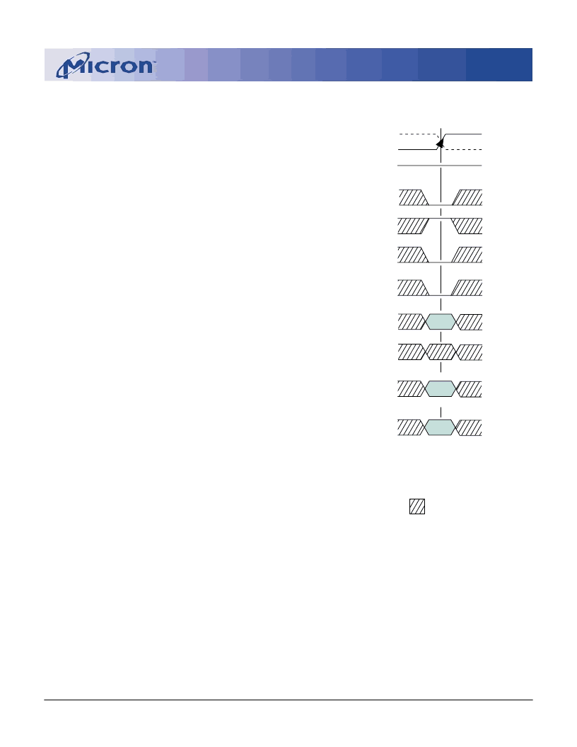
Figure 14
WRITE Command
Data for any WRITE burst may be followed by a
subsequent PRECHARGE command. To follow a WRITE
without truncating the WRITE burst,
t
WR should be
met as shown in Figure 22.
Data for any WRITE burst may be truncated by a
subsequent PRECHARGE command, as shown in Fig-
ures 23 and 24. Note that only the data-in pairs that are
registered prior to the
t
WR period are written to the
internal array, and any subsequent data-in should be
masked with DM as shown in Figures 23 and 24. After
the PRECHARGE command, a subsequent command
to the same bank cannot be issued until
t
RP is met.
CS#
WE#
CAS#
RAS#
CKE
CA
A8
BA0,1
HIGH
EN AP
DIS AP
BA
CK
CK#
CA = Column Address
BA = Bank Address
EN AP = Enable Auto Precharge
DIS AP = Disable Auto Precharge
DON T CARE
A0-A7
A9, A10, A11
相關(guān)PDF資料 |
PDF描述 |
|---|---|
| MT46V64M4 | 16 Meg x 4 x 4 banks DDR SDRAM(16M x 4 x 4組,雙數(shù)據(jù)速率同步動態(tài)RAM) |
| MT46V64M8 | 16 Meg x 8 x 4 banks DDR SDRAM(16M x 8 x 4組,雙數(shù)據(jù)速率同步動態(tài)RAM) |
| MT48LC16M8A1TG | SYNCHRONOUS DRAM |
| MT48LC32M4A1 | ECONOLINE: RSZ/P - 1kVDC |
| MT48LC32M4A2 | SYNCHRONOUS DRAM |
相關(guān)代理商/技術(shù)參數(shù) |
參數(shù)描述 |
|---|---|
| MT46V64M16 | 制造商:MICRON 制造商全稱:Micron Technology 功能描述:DOUBLE DATA RATE (DDR) SDRAM |
發(fā)布緊急采購,3分鐘左右您將得到回復(fù)。