- 您現(xiàn)在的位置:買(mǎi)賣(mài)IC網(wǎng) > PDF目錄385639 > MT46V2M32V1 (Micron Technology, Inc.) DOUBLE DATA RATE DDR SDRAM PDF資料下載
參數(shù)資料
| 型號(hào): | MT46V2M32V1 |
| 廠商: | Micron Technology, Inc. |
| 英文描述: | DOUBLE DATA RATE DDR SDRAM |
| 中文描述: | 雙倍數(shù)據(jù)速率的DDR SDRAM內(nèi)存 |
| 文件頁(yè)數(shù): | 63/65頁(yè) |
| 文件大?。?/td> | 2360K |
| 代理商: | MT46V2M32V1 |
第1頁(yè)第2頁(yè)第3頁(yè)第4頁(yè)第5頁(yè)第6頁(yè)第7頁(yè)第8頁(yè)第9頁(yè)第10頁(yè)第11頁(yè)第12頁(yè)第13頁(yè)第14頁(yè)第15頁(yè)第16頁(yè)第17頁(yè)第18頁(yè)第19頁(yè)第20頁(yè)第21頁(yè)第22頁(yè)第23頁(yè)第24頁(yè)第25頁(yè)第26頁(yè)第27頁(yè)第28頁(yè)第29頁(yè)第30頁(yè)第31頁(yè)第32頁(yè)第33頁(yè)第34頁(yè)第35頁(yè)第36頁(yè)第37頁(yè)第38頁(yè)第39頁(yè)第40頁(yè)第41頁(yè)第42頁(yè)第43頁(yè)第44頁(yè)第45頁(yè)第46頁(yè)第47頁(yè)第48頁(yè)第49頁(yè)第50頁(yè)第51頁(yè)第52頁(yè)第53頁(yè)第54頁(yè)第55頁(yè)第56頁(yè)第57頁(yè)第58頁(yè)第59頁(yè)第60頁(yè)第61頁(yè)第62頁(yè)當(dāng)前第63頁(yè)第64頁(yè)第65頁(yè)
63
64Mb: x32 DDR SDRAM
2M32DDR-07.p65
–
Rev. 12/01
Micron Technology, Inc., reserves the right to change products or specifications without notice.
2001, Micron Technology, Inc.
64Mb: x32
DDR SDRAM
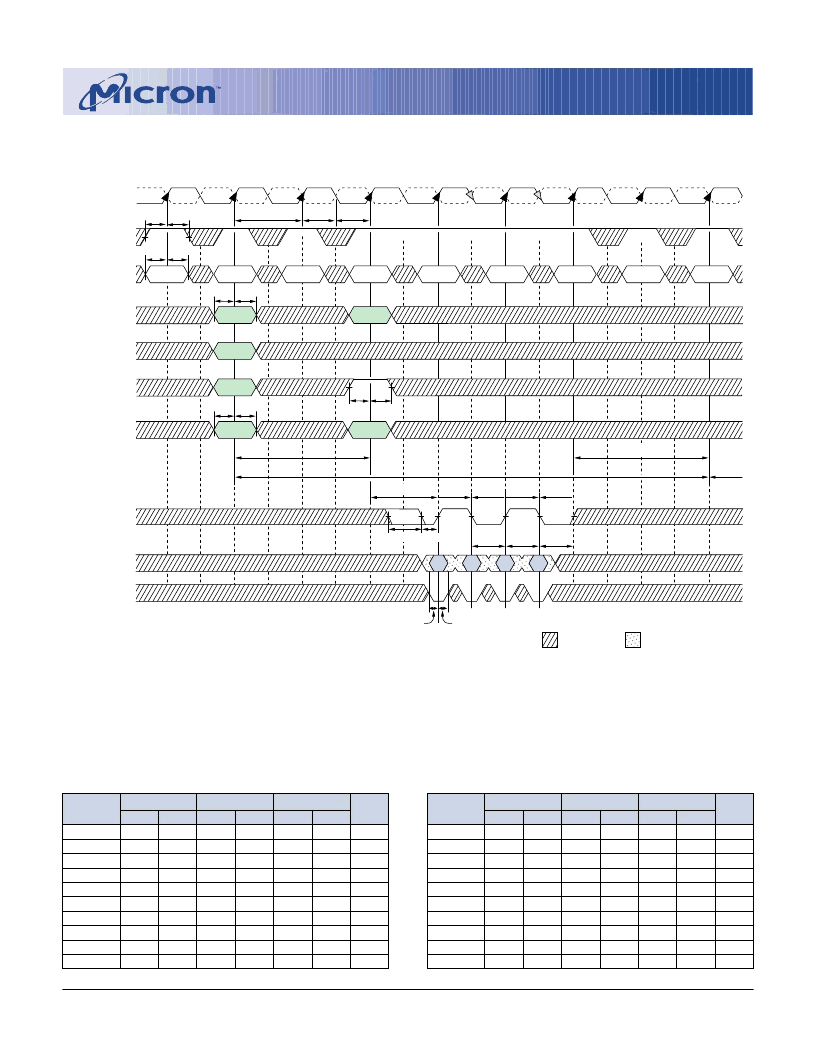
BANK WRITE
–
WITH AUTO PRECHARGE
TIMING PARAMETERS
-5
-6
-65
SYMBOL
t
CH
t
CL
t
CK (3)
t
CK (2)
t
DH
t
DS
t
DQSH
t
DQSL
t
DQSS
t
DSS
MIN
0.45
0.45
5
8
0.6
0.6
0.4
0.4
0.75
0.25
MAX
0.55
0.55
12
12
MIN
0.45
0.45
6
9
0.6
0.6
0.4
0.4
0.75
0.25
MAX
0.55
0.55
12
12
MIN
0.45
0.45
6.5
10
0.6
0.6
0.4
0.4
0.75
0.25
MAX
0.55
0.55
12
12
UNITS
t
CK
t
CK
ns
ns
ns
ns
t
CK
t
CK
t
CK
t
CK
1.25
1.25
1.25
-5
-6
-65
SYMBOL
t
DSH
t
IH
t
IS
t
RAS
t
RCD
t
RP
t
WPRE
t
WPRES
t
WPST
t
WR
MIN
0.25
1
1
40
20
20
0.25
0
0.4
2
MAX
MIN
0.25
1
1
40
18
18
0.25
0
0.4
2
MAX
MIN
0.25
1
1
40
19.5
19.5
025
0
0.4
2
MAX
UNITS
t
CK
ns
ns
ns
ns
ns
t
CK
ns
t
CK
t
CK
120,000
120,000
120,000
0.6
0.6
0.6
CK
CK#
CKE
A8
BA0, BA1
t
CK
t
CH
tCL
t
IS
t
IS
t
IH
t
IS
t
IS
t
IH
t
IH
t
IH
t
IS
t
IH
RA
t
RCD
t
RAS
t
DSH
6
t
RP
t
WR
T0
T1
T2
T3
T4
T5
T5n
T6
T7
T8
T4n
A0-A7
A9, A10
NOTE:
1. DI
n
= data-out from column
n
; subsequent elements are provided in the programmed order.
2. Burst length = 4 in the case shown.
3. Enable auto precharge.
4. ACT = ACTIVE, RA = Row Address, BA = Bank Address.
5. NOP commands are shown for ease of illustration; other commands may be valid at these times.
6.tDSH is applicable during tDQSS(MIN)
and is referenced from CK T4 or T5.
7.tDSS is applicable during tDQSS (MAX)
and is referenced from CK T5 or T6.
NOP5
NOP5
COMMAND
4
3
ACT
RA
RA
Col
n
WRITE2
NOP5
Bank
x
NOP5
Bank
x
NOP5
NOP5
NOP5
t
DQSL
t
DQSH
t
WPST
t
DSS
7
t
DSH
6
t
DSS
7
DQ
1
DQS
DM
DI
b
t
DS
t
DH
t
DQSS (NOM)
DON
’
T CARE
TRANSITIONING DATA
t
WPRES
t
WPRE
相關(guān)PDF資料 |
PDF描述 |
|---|---|
| MT46V32M4-1 | DOUBLE DATA RATE DDR SDRAM |
| MT46V32M4TG-75 | DOUBLE DATA RATE DDR SDRAM |
| MT46V32M4TG-75L | DOUBLE DATA RATE DDR SDRAM |
| MT46V32M4TG-75Z | DOUBLE DATA RATE DDR SDRAM |
| MT46V32M4TG-75ZL | DOUBLE DATA RATE DDR SDRAM |
相關(guān)代理商/技術(shù)參數(shù) |
參數(shù)描述 |
|---|---|
| MT46V32M16 | 制造商:Micron Technology Inc 功能描述:32MX16 DDR SDRAM PLASTIC IND TEMP BGA 2.6V DDR - Trays |
| MT46V32M16-5B | 制造商:Micron Technology Inc 功能描述: |
發(fā)布緊急采購(gòu),3分鐘左右您將得到回復(fù)。