- 您現(xiàn)在的位置:買賣IC網(wǎng) > PDF目錄384755 > MT16LSDT6464A (Micron Technology, Inc.) SYNCHRONOUS DRAM MODULE PDF資料下載
參數(shù)資料
| 型號: | MT16LSDT6464A |
| 廠商: | Micron Technology, Inc. |
| 英文描述: | SYNCHRONOUS DRAM MODULE |
| 中文描述: | 同步DRAM模塊 |
| 文件頁數(shù): | 19/24頁 |
| 文件大?。?/td> | 614K |
| 代理商: | MT16LSDT6464A |
256MB / 512MB (x64)
168-PIN SDRAM DIMMs
32,64 Meg x 64 SDRAM DIMMs
SD8_16C32_64x64AG_C.fm - Rev. C 11/02
Micron Technology, Inc., reserves the right to change products or specifications without notice.
19
2002, Micron Technology Inc.
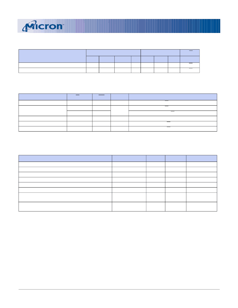
Table 18: EEPROM Device Select Code
The most significant bit (b7) is sent first
DEVICE TYPE IDENTIFIER
CHIP ENABLE
RW
b7
b6
b5
b4
b3
b2
b1
b0
Memory Area Select Code (two arrays)
Protection Register Select Code
1
0
0
1
1
1
0
0
SA2
SA2
SA1
SA1
SA0
SA0
RW
RW
Table 19: EEPROM Operating Modes
MODE
RW BIT
WC
BYTES
INITIAL SEQUENCE
Current Address Read
RandomAddressRead
1
0
1
1
0
0
V
IH
or V
IL
V
IH
or V
IL
V
IH
or V
IL
V
IH
or V
IL
V
IL
V
IL
1
Start, Device Select, RW = 1
Start, Device Select, RW= 0, Address
RESTART, Device Select, RW= 1
Similar to Current or Random Address Read
START, Device Select, RW = 0
START, Device Select, RW = 0
1
Sequential Read
Byte Write
Page Write
1
1
16
Table 20: SERIAL Presence-Detect EEPROM DC Operating Conditions
V
DD
= +3.3V ±0.3V; All voltages referenced to V
SS
PARAMETER/CONDITION
SYMBOL
MIN
MAX
UNITS
SUPPLY VOLTAGE
INPUT HIGH VOLTAGE: Logic 1; All inputs
INPUT LOW VOLTAGE: Logic 0; All inputs
OUTPUT LOW VOLTAGE: I
OUT
= 3mA
INPUT LEAKAGE CURRENT: V
IN
= GND to V
DD
OUTPUT LEAKAGE CURRENT: V
OUT
= GND to V
DD
STANDBY CURRENT: SCL = SDA = V
DD
- 0.3V; All other
inputs = GND or 3.3V ±10%
POWER SUPPLY CURRENT:
SCL Clock frequency = 100 KHz
V
DD
V
IH
V
IL
V
OL
I
LI
I
LO
I
CCS
3
3.6
V
V
V
V
V
DD
x 0.7
-1
–
–
–
–
V
DD
+ 0.5
V
DD
x 0.3
0.4
10
10
30
μA
μA
μA
I
CC
Write
I
CC
Read
–
–
3
1
mA
發(fā)布緊急采購,3分鐘左右您將得到回復。