- 您現(xiàn)在的位置:買賣IC網(wǎng) > PDF目錄25640 > MSP430F2013TRSAR (TEXAS INSTRUMENTS INC) 16-BIT, FLASH, 16 MHz, RISC MICROCONTROLLER, PQCC16 PDF資料下載
參數(shù)資料
| 型號: | MSP430F2013TRSAR |
| 廠商: | TEXAS INSTRUMENTS INC |
| 元件分類: | 微控制器/微處理器 |
| 英文描述: | 16-BIT, FLASH, 16 MHz, RISC MICROCONTROLLER, PQCC16 |
| 封裝: | GREEN, PLASTIC, QFN-16 |
| 文件頁數(shù): | 49/92頁 |
| 文件大小: | 1672K |
| 代理商: | MSP430F2013TRSAR |
第1頁第2頁第3頁第4頁第5頁第6頁第7頁第8頁第9頁第10頁第11頁第12頁第13頁第14頁第15頁第16頁第17頁第18頁第19頁第20頁第21頁第22頁第23頁第24頁第25頁第26頁第27頁第28頁第29頁第30頁第31頁第32頁第33頁第34頁第35頁第36頁第37頁第38頁第39頁第40頁第41頁第42頁第43頁第44頁第45頁第46頁第47頁第48頁當(dāng)前第49頁第50頁第51頁第52頁第53頁第54頁第55頁第56頁第57頁第58頁第59頁第60頁第61頁第62頁第63頁第64頁第65頁第66頁第67頁第68頁第69頁第70頁第71頁第72頁第73頁第74頁第75頁第76頁第77頁第78頁第79頁第80頁第81頁第82頁第83頁第84頁第85頁第86頁第87頁第88頁第89頁第90頁第91頁第92頁
MSP430F20x3
MSP430F20x2
MSP430F20x1
SLAS491H
– AUGUST 2005 – REVISED AUGUST 2011
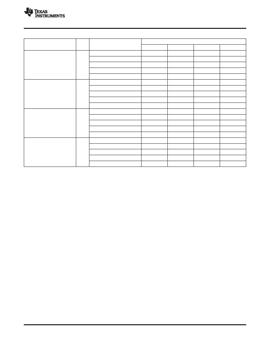
Table 20. Port P1 (P1.4 to P1.7) Pin Functions, MSP430F20x1
CONTROL BITS / SIGNALS(2)
PIN NAME (P1.x)
x
FUNCTION(1)
P1DIR.x
P1SEL.x
CAPD.x
JTAG Mode
P1.4(3) input/output
0/1
0
N/A
0
1
0
P1.4/SMCLK/CA4/TCK
4
SMCLK
1
0
CA4(4)
X
1
0
TCK(5)
X
1
P1.5(3) input/output
0/1
0
N/A
0
1
0
P1.5/TA0/CA5/TMS
5
Timer_A2.TA0
1
0
CA5(4)
X
1
0
TMS(5)
X
1
P1.6(3) input/output
0/1
0
N/A
0
1
0
P1.6/TA1/CA6/TDI
6
Timer_A2.TA1
1
0
CA6(4)
X
1
0
TDI(5)
X
1
P1.7(3) input/output
0/1
0
N/A
0
1
0
P1.7/CAOUT/CA7/TDO/TDI
7
CAOUT
1
0
CA7(4)
X
1
0
TDO/TDI(5)(6)
X
1
(1)
N/A = Not available or not applicable
(2)
X = Don
't care
(3)
Default after reset (PUC/POR)
(4)
Setting the CAPD.x bit disables the output driver as well as the input Schmitt trigger to prevent parasitic cross currents when applying
analog signals. Selecting the CAx input pin to the comparator multiplexer with the P2CAx bits automatically disables the input buffer for
that pin, regardless of the state of the associated CAPD.x bit.
(5)
In JTAG mode the internal pullup/down resistors are disabled.
(6)
Function controlled by JTAG
Copyright
2005–2011, Texas Instruments Incorporated
53
發(fā)布緊急采購,3分鐘左右您將得到回復(fù)。