- 您現(xiàn)在的位置:買賣IC網(wǎng) > PDF目錄378018 > MSM7715 (OKI SEMICONDUCTOR CO., LTD.) Multi-Function Telecommunication LSI PDF資料下載
參數(shù)資料
| 型號: | MSM7715 |
| 廠商: | OKI SEMICONDUCTOR CO., LTD. |
| 英文描述: | Multi-Function Telecommunication LSI |
| 中文描述: | 多功能通信大規(guī)模集成電路 |
| 文件頁數(shù): | 7/21頁 |
| 文件大小: | 150K |
| 代理商: | MSM7715 |
Semiconductor
MSM7715
7/21
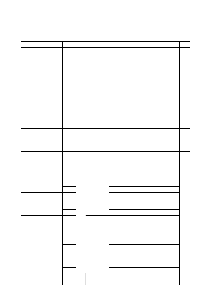
Parameter
Min.
–16.5
–15.5
Unit
dBm
*1
V
DTTL
V
DTTH
Transmit Level
Condition
Symbol
Typ.
–14.5
–13.5
Max.
–12.5
–11.5
V
DTDF
f
DDT
THD
DT
t
SDT
0
–1.5
—
dB
ns
Low-group tone
High-group tone
DTTIM = "1"
DTTIM = "0"
DTTIM = "1"
DTTIM = "0"
DTTIM = "1"
DTTIM = "0"
DTTIM = "1"
DTTIM = "0"
DTTIM = "1"
DTTIM = "0"
High-group tone/low-group tone
AOUT, R1 = R3
With respect to the nominal frequency
Harmonics/Fundamental frequency
See Fig. 2.
(
V
DD
= 2.5 V to 3.6 V, Ta = –40°C to +85°C)
Transmit Signal Level
Relative Value
Transmit Frequency
Deviation
Transmit Signal
Distortion Rate
DTG1 to DTG4 Input Data
Setup Time
DTG1 to DTG4 Input Data
Hold Time
Receive Detect Level
Receive Reject Level
Receive Frequency
Detect Band
Receive Frequency
Reject Band
Allowable Receive Level
Difference
Allowable Receive
Noise Level ratio
Dial Tone Reject Ratio
Signal Repetition Time
Tone Time for Detect
Tone Time for No Detect
Output Delay Time
Interdigit Pause Time
Acceptable Drop Out Time
SP Delay Time
Output Trailing Edge
Delay Time
t
HDT
See Fig. 2.
V
DETDT
V
REJDT
For each single tone
For each single tone
f
DETDT
With respect to the nominal frequency
f
REJDT
With respect to the nominal frequency
V
TWIST
High-group tone/low-group tone
V
N/S
Noise (0.3 kHz to 3.4 kHz)
level/tone level
380 Hz to 420 Hz
V
REJ400
t
C1
t
C2
t
S1
t
S2
t
I1
t
I2
t
G11
t
G12
t
G21
t
G22
t
P1
t
P2
t
B1
t
B2
t
SP1
t
SP2
t
D1
t
D2
DTTIM = "1"
DTTIM = "0"
DTTIM = "1"
DTTIM = "0"
DTTIM = "1"
DTTIM = "0"
DTTIM = "1"
DTTIM = "0"
250
250
–46
—
—
±3.8
–6
—
37
120
70
49
34
—
—
30
20
30
20
30
21
—
—
6
1
21
15
1
—
—
—
—
—
—
—
—
—
–12
—
—
—
—
—
—
—
45
32
48
35
—
—
—
—
8
1.7
29
21
2
+1.5
–23
—
—
–10
–60
±1.5
—
+6
—
—
—
—
—
—
24
9
57
42
77
62
—
—
10
3
10
3
35
27
%
dB
dBm
*1
%
dB
ms
t
S
> 80 ms
t
S
> 44 ms
See Fig. 1
Normal
condition *2
Just after
mode change *3
AC Characteristics (DTMF)
相關(guān)PDF資料 |
PDF描述 |
|---|---|
| MSM7728 | Single Rail Linear CODEC |
| MSM7731-01 | Multifunction PCM CODEC (Voice Signal Processor) |
| MSM7731-02 | Dual Echo Canceler & Noise Canceler with Dual Codec for Hands-Free |
| MSM80C154S | CMOS 8-bit Microcontroller |
| MSM83C154S | Electrical, Duct/Raceway (Trunking); |
相關(guān)代理商/技術(shù)參數(shù) |
參數(shù)描述 |
|---|---|
| MSM7715GS-2K | 制造商:ROHM Semiconductor 功能描述: |
| MSM7716 | 制造商:OKI 制造商全稱:OKI electronic componets 功能描述:Single Rail Linear CODEC |
| MSM7716GSK | 制造商:ROHM Semiconductor 功能描述: |
| MSM7716GS-K | 制造商:OKI 制造商全稱:OKI electronic componets 功能描述:Single Rail Linear CODEC |
| MSM7716GS-KR1 | 制造商:ROHM Semiconductor 功能描述: |
發(fā)布緊急采購,3分鐘左右您將得到回復(fù)。