- 您現(xiàn)在的位置:買賣IC網(wǎng) > PDF目錄224504 > MSM548128BL-70GS-K (OKI ELECTRIC INDUSTRY CO LTD) 128K X 8 PSEUDO STATIC RAM, 70 ns, PDSO32 PDF資料下載
參數(shù)資料
| 型號(hào): | MSM548128BL-70GS-K |
| 廠商: | OKI ELECTRIC INDUSTRY CO LTD |
| 元件分類: | SRAM |
| 英文描述: | 128K X 8 PSEUDO STATIC RAM, 70 ns, PDSO32 |
| 封裝: | 0.525 INCH, 1.27 MM PITCH, PLASTIC, SOP-32 |
| 文件頁(yè)數(shù): | 9/12頁(yè) |
| 文件大小: | 182K |
| 代理商: | MSM548128BL-70GS-K |
Semiconductor
MSM548128BL
6/12
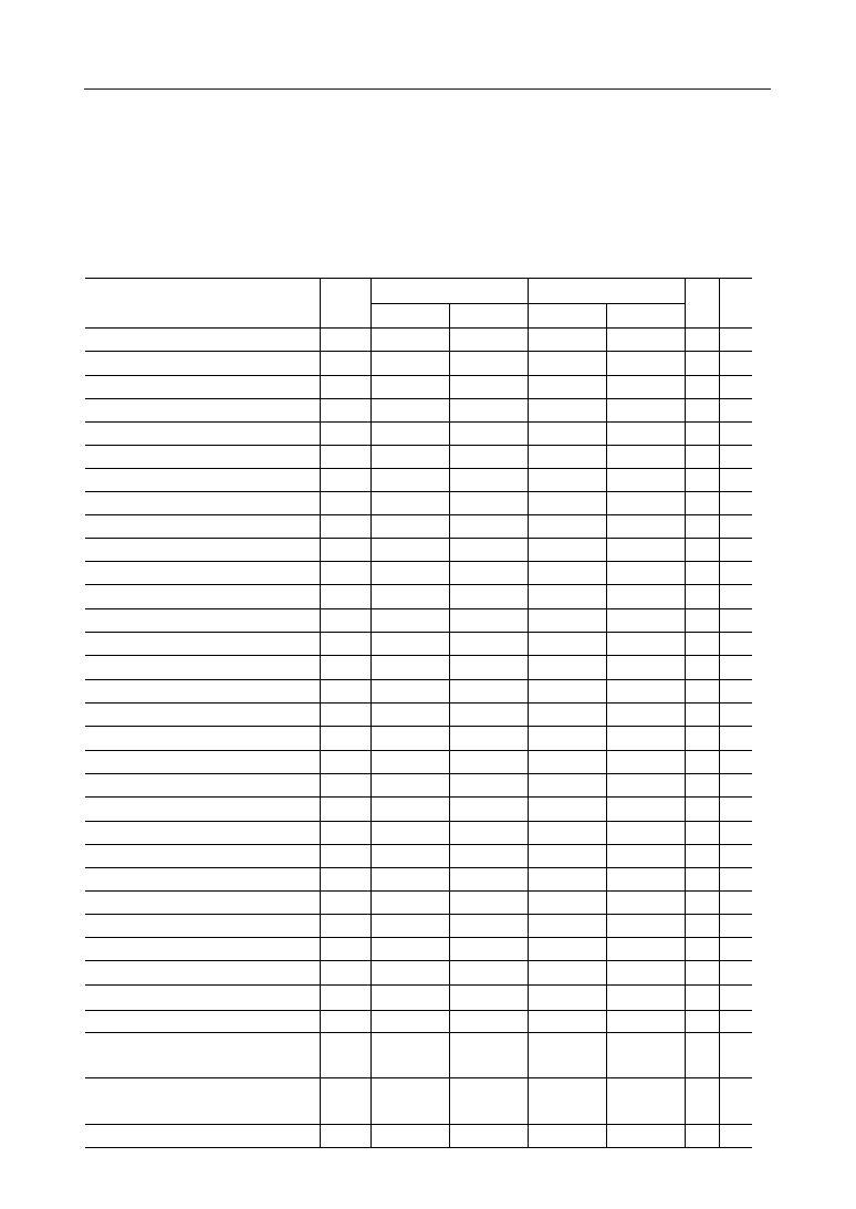
AC Characteristics
Measurement condition:
Input pulse level ........................... VIH = 2.4 V, VIL = 0.4 V
Output reference level .................. VOH = 2.0 V, VOL = 0.8 V
Rising and falling time ................. 5 ns
Output load .................................... 1 TTL + 100 pF
Input timing reference level ........ High = 2.2 V, Low = 0.8 V
Parameter
Symbol
Note
tRC
Random Read Write Cycle Time
Unit
ns
MSM548128BL-80
130
Max.
Min.
—
MSM548128BL-70
120
Max.
Min.
—
tRWC
Random Read Modify Write Cycle Time
ns
190
—
170
—
tCEA
CE Access Time
ns
—80
—70
tOEA
OE Access Time
ns
—30
tCHZ
Chip Disable to Output in High-Z
6
ns
—30
tCLZ
CE to Output in Low-Z
ns
25
—
25
—
tOHZ
OE Disable to Output in High-Z
6
ns
—25
—20
tOLZ
OE Output in Low-Z
ns
0—
tCE
CE Pulse Width
s
80n
10m
70n
10m
tP
CE Precharge Time
ns
40
—
40
—
tAS
Address Set-up Time
ns
0—
tAH
Address Hold Time
ns
30
—
25
—
tRCS
Read Command Set-up Time
ns
0—
tRCH
Read Command Hold Time
ns
0—
tWP
Write Command Pulse Width
ns
30
—
25
—
tCW
Chip Enable Time
ns
80
—
70
—
tDW
Input Data Set-up Time
ns
25
—
25
—
tDH
Input Data Hold Time
ns
0—
tOW
Output Active from End of Write
ns
5—
tWHZ
Write Enable to Output in High-Z
6
ns
—25
—20
tT
Transition Time
11
ns
350
tRFD
RFSH Delay Time from CE
ns
40
—
40
—
tFP
RFSH Precharge Time
ns
30
—
30
—
tFAP
RFSH Pulse Width (Auto-refresh)
s
30n
8m
30n
8m
tFC
Auto-refresh Cycle Time
ns
130
—
120
—
tRHC
RFSH Command Hold Time
ns
15
—
15
—
tRCD
RFSH Delay Time (Standby Mode)
ns
—5
tCSS
CS Set-up Time
ns
0—
tCSH
CS Hold Time
ns
30
—
25
—
tFAS
RFSH Pulse Width (Self-refresh)
ms
8—
tRFS
CE Delay Time from RFSH
in Self-refresh Mode
ns
160
—
150
—
tRFA
CE Delay Time from RFSH
in Auto-refresh Mode
ns
0—
tREF
Refresh Period (512 cycle/8 ms)
ms
—8
(VCC = 5 V ±10%, Ta = 0°C to 70°C)
相關(guān)PDF資料 |
PDF描述 |
|---|---|
| MSMD | FEMALE; MALE, D SUBMINIATURE CONNECTOR, SURFACE MOUNT, PLUG; SOCKET |
| MSMSOJ-24-.4-T-L | SOJ24, IC SOCKET |
| MSMSOJ-24-.3-T-L | SOJ24, IC SOCKET |
| MSMSOJ-42-.4-T-X | SOJ42, IC SOCKET |
| MSMSOJ-40-.4-T-L | SOJ40, IC SOCKET |
相關(guān)代理商/技術(shù)參數(shù) |
參數(shù)描述 |
|---|---|
| MSM548262-60JS | 制造商:ROHM Semiconductor 功能描述: |
| MSM548262-60T3-K | 制造商:ROHM Semiconductor 功能描述: |
| MSM548262-60TK | 制造商:OK International 功能描述: |
| MSM548262-60TS-K | 制造商:ROHM Semiconductor 功能描述: |
| MSM548262-70JS | 制造商:ROHM Semiconductor 功能描述: |
發(fā)布緊急采購(gòu),3分鐘左右您將得到回復(fù)。