- 您現(xiàn)在的位置:買賣IC網(wǎng) > PDF目錄45388 > MSC1213Y4PAGRG4 (TEXAS INSTRUMENTS INC) 8-BIT, FLASH, 40 MHz, MICROCONTROLLER, PQFP64 PDF資料下載
參數(shù)資料
| 型號: | MSC1213Y4PAGRG4 |
| 廠商: | TEXAS INSTRUMENTS INC |
| 元件分類: | 微控制器/微處理器 |
| 英文描述: | 8-BIT, FLASH, 40 MHz, MICROCONTROLLER, PQFP64 |
| 封裝: | GREEN, PLASTIC, TQFP-64 |
| 文件頁數(shù): | 39/111頁 |
| 文件大小: | 1102K |
| 代理商: | MSC1213Y4PAGRG4 |
第1頁第2頁第3頁第4頁第5頁第6頁第7頁第8頁第9頁第10頁第11頁第12頁第13頁第14頁第15頁第16頁第17頁第18頁第19頁第20頁第21頁第22頁第23頁第24頁第25頁第26頁第27頁第28頁第29頁第30頁第31頁第32頁第33頁第34頁第35頁第36頁第37頁第38頁當前第39頁第40頁第41頁第42頁第43頁第44頁第45頁第46頁第47頁第48頁第49頁第50頁第51頁第52頁第53頁第54頁第55頁第56頁第57頁第58頁第59頁第60頁第61頁第62頁第63頁第64頁第65頁第66頁第67頁第68頁第69頁第70頁第71頁第72頁第73頁第74頁第75頁第76頁第77頁第78頁第79頁第80頁第81頁第82頁第83頁第84頁第85頁第86頁第87頁第88頁第89頁第90頁第91頁第92頁第93頁第94頁第95頁第96頁第97頁第98頁第99頁第100頁第101頁第102頁第103頁第104頁第105頁第106頁第107頁第108頁第109頁第110頁第111頁

MSC1211, MSC1212
MSC1213,MSC1214
SBAS323G JUNE 2004 REVISED OCTOBER 2007
www.ti.com
33
MEMORY MAP
The MSC1211/12/13/14 contain on-chip SFR, Flash
Memory, Scratchpad SRAM Memory, Boot ROM, and
SRAM. The SFR registers are primarily used for control
and status. The standard 8051 features and additional
peripheral
features
of
the
MSC1211/12/13/14
are
controlled through the SFR. Reading from an undefined
SFR will return zero; writing to an undefined SFR is not
recommended, and will have indeterminate effects.
Flash Memory is used for both Program Memory and Data
Memory. The user has the ability to select the partition size
of Program and Data Memory. The partition size is set
through
hardware
configuration
bits,
which
are
programmed
through
either
the
parallel
or
serial
programming methods. Both Program and Data Flash
Memory are erasable and writable (programmable) in User
Application mode (UAM). However, program execution
can only occur from Program Memory. As an added
precaution, a lock feature can be activated through the
hardware configuration bits, which disables erase and
writes to 4kB of Program Flash Memory or the entire
Program Flash Memory in UAM.
The MSC1211/12/13/14 include 1kB of SRAM on-chip.
SRAM starts at address 0 and is accessed through the
MOVX instruction. This SRAM can also be located to start
at 8400h and can be accessed as both Program and Data
Memory.
FLASH MEMORY
The page size for Flash memory is 128 bytes. The
respective page must be erased before it can be written to,
regardless of whether it is mapped to Program or Data
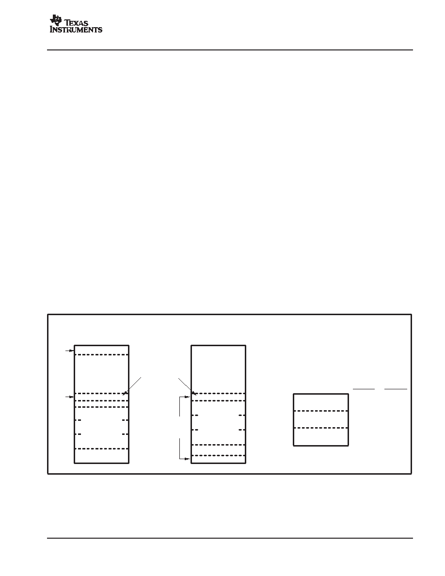
Memory space. The MSC1211/12/13/14 use a memory
addressing scheme that separates Program Memory
(FLASH/ROM) from Data Memory (FLASH/RAM). Each
area is 64kB beginning at address 0000h and ending at
FFFFh, as shown in Figure 20. The program and data
segments can overlap since they are accessed in different
ways. Program Memory is fetched by the microcontroller
automatically. There is one instruction (MOVC) that is
used to explicitly read the program area. This instruction
is commonly used to read lookup tables. The Data Memory
area is accessed explicitly using the MOVX instruction.
This instruction provides multiple ways of specifying the
target address. It is also used to access the 64kB of Data
Memory. The address and data range of devices with
on-chip Program and Data Memory overlap the 64kB
memory space. When on-chip memory is enabled,
accessing memory in the on-chip range will cause the
device to access internal memory. Memory accesses
beyond the internal range will be addressed externally via
Ports 0 and 2.
The MSC1211/12/13/14 have two hardware configuration
registers (HCR0 and HCR1) that are programmable only
during Flash Memory Programming mode.
1k RAM or External
External Memory
S
e
le
ct
in
MC
O
N
Se
le
ct
in
H
CR0
0000h, 0k
1FFFh, 8k (Y3)
0FFFh, 4k (Y2)
3FFFh, 16k (Y4)
8400h
7FFFh, 32k (Y5)
2k Internal Boot ROM
F800h
FFFFh
External
Program
Memory
Mapped to Both
Memory Spaces
(von Neumann)
8800h
Se
le
ct
in
MC
O
N
03FFh, 1k
13FFh, 5k (Y2)
23FFh, 9k (Y3)
43FFh, 17k (Y4)
83FFh, 33k (Y5)
FFFFh
External
Data
Memory
Program
Memory
Data
Memory
8800h
OnChip
Flash
OnChip
Flash
Programming
Mode
Address
User
Application
Mode
Address(1)
NOTE: (1) Can be accessed using CADDR
or the faddr_data_read Boot ROM routine.
UAM: Read Only
FPM: Read Only
UAM: Read Only
FPM: Read/Write
UAM: Read Only
FPM: Read/Write
807Fh
8000h
8070h
7Fh
8079h
79h
00h
70h
Configuration
Memory
Figure 20. Memory Map
相關(guān)PDF資料 |
PDF描述 |
|---|---|
| MSC1214Y3PAGRG4 | 8-BIT, FLASH, 40 MHz, MICROCONTROLLER, PQFP64 |
| MSC1214Y2PAGTG4 | 8-BIT, FLASH, 40 MHz, MICROCONTROLLER, PQFP64 |
| MSC1214Y2PAGR | 8-BIT, FLASH, 40 MHz, MICROCONTROLLER, PQFP64 |
| MSC1212Y3PAGR | 8-BIT, FLASH, 40 MHz, MICROCONTROLLER, PQFP64 |
| MSC1211Y2PAGR | 8-BIT, FLASH, 40 MHz, MICROCONTROLLER, PQFP64 |
相關(guān)代理商/技術(shù)參數(shù) |
參數(shù)描述 |
|---|---|
| MSC1213Y4PAGT | 功能描述:數(shù)據(jù)轉(zhuǎn)換系統(tǒng) Prec A/D & D/A w/ 8051 Mcntrl & Flash RoHS:否 制造商:Texas Instruments 轉(zhuǎn)換速率:0.001 MSPs 分辨率:24 bit 最大工作溫度:+ 125 C 最小工作溫度:- 40 C 安裝風格:SMD/SMT 封裝 / 箱體:TQFP-64 封裝:Reel |
| MSC1213Y4PAGTG4 | 功能描述:數(shù)據(jù)轉(zhuǎn)換系統(tǒng) Prec A/D D/A w/8051 Microcntrlr & Fl Mem RoHS:否 制造商:Texas Instruments 轉(zhuǎn)換速率:0.001 MSPs 分辨率:24 bit 最大工作溫度:+ 125 C 最小工作溫度:- 40 C 安裝風格:SMD/SMT 封裝 / 箱體:TQFP-64 封裝:Reel |
| MSC1213Y5 | 制造商:TI 制造商全稱:Texas Instruments 功能描述:Precision Analog-to-Digital Converter (ADC) and Digital-to-Analog Converters (DACs) with 8051 Microcontroller and Flash Memory |
| MSC1213Y5PAGR | 功能描述:數(shù)據(jù)轉(zhuǎn)換系統(tǒng) Prec A/D & D/A w/ 8051 Mcntrl & Flash RoHS:否 制造商:Texas Instruments 轉(zhuǎn)換速率:0.001 MSPs 分辨率:24 bit 最大工作溫度:+ 125 C 最小工作溫度:- 40 C 安裝風格:SMD/SMT 封裝 / 箱體:TQFP-64 封裝:Reel |
| MSC1213Y5PAGRG4 | 功能描述:數(shù)據(jù)轉(zhuǎn)換系統(tǒng) Prec A/D & D/A with 8051 MCU and FL Mem RoHS:否 制造商:Texas Instruments 轉(zhuǎn)換速率:0.001 MSPs 分辨率:24 bit 最大工作溫度:+ 125 C 最小工作溫度:- 40 C 安裝風格:SMD/SMT 封裝 / 箱體:TQFP-64 封裝:Reel |
發(fā)布緊急采購,3分鐘左右您將得到回復(fù)。