- 您現(xiàn)在的位置:買賣IC網(wǎng) > PDF目錄359219 > MRF7S19100NBR1 (飛思卡爾半導(dǎo)體(中國)有限公司) RF Power Field Effect Transistors N-Channel Enhancement-Mode Lateral MOSFETs PDF資料下載
參數(shù)資料
| 型號: | MRF7S19100NBR1 |
| 廠商: | 飛思卡爾半導(dǎo)體(中國)有限公司 |
| 英文描述: | RF Power Field Effect Transistors N-Channel Enhancement-Mode Lateral MOSFETs |
| 中文描述: | 射頻功率場效應(yīng)晶體管N溝道增強型MOSFET的外側(cè) |
| 文件頁數(shù): | 2/15頁 |
| 文件大?。?/td> | 544K |
| 代理商: | MRF7S19100NBR1 |
2
RF Device Data
Freescale Semiconductor
MRF7S19100NR1 MRF7S19100NBR1
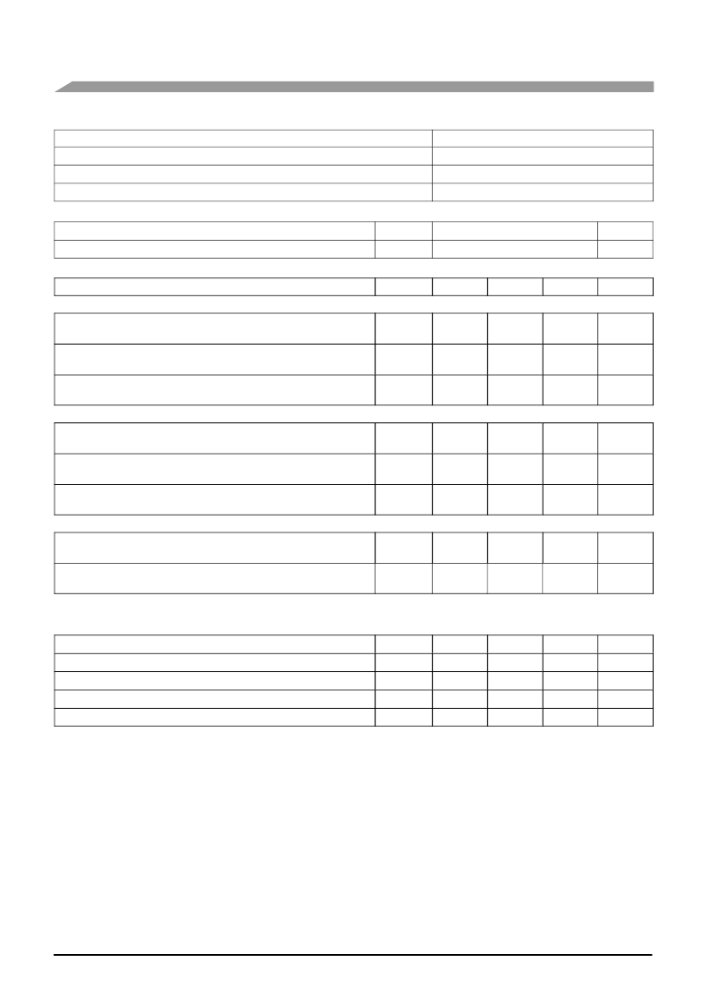
Table 3. ESD Protection Characteristics
Test Methodology
Class
Human Body Model (per JESD22-A114)
1C (Minimum)
Machine Model (per EIA/JESD22-A115)
A (Minimum)
Charge Device Model (per JESD22-C101)
IV (Minimum)
Table 4. Moisture Sensitivity Level
Test Methodology
Rating
Package Peak Temperature
Unit
Per JESD 22-A113, IPC/JEDEC J-STD-020
3
260
°
C
Table 5. Electrical Characteristics
(T
C
= 25
°
C unless otherwise noted)
Characteristic
Symbol
Min
Typ
Max
Unit
Off Characteristics
Zero Gate Voltage Drain Leakage Current
(V
DS
= 65 Vdc, V
GS
= 0 Vdc)
I
DSS
—
—
10
μ
Adc
Zero Gate Voltage Drain Leakage Current
(V
DS
= 28 Vdc, V
GS
= 0 Vdc)
I
DSS
—
—
1
μ
Adc
Gate-Source Leakage Current
(V
GS
= 5 Vdc, V
DS
= 0 Vdc)
I
GSS
—
—
500
nAdc
On Characteristics
Gate Threshold Voltage
(V
DS
= 10 Vdc, I
D
= 320
μ
Adc)
V
GS(th)
1
2
3
Vdc
Gate Quiescent Voltage
(1)
(V
DS
= 28 Vdc, I
D
= 1000 mAdc, Measured in Functional Test)
V
GS(Q)
2
2.8
4
Vdc
Drain-Source On-Voltage
(V
GS
= 10 Vdc, I
D
= 3.2 Adc)
V
DS(on)
0.2
0.24
0.4
Vdc
Dynamic Characteristics
(2)
Reverse Transfer Capacitance
(V
DS
= 28 Vdc
±
30 mV(rms)ac @ 1 MHz, V
GS
= 0 Vdc)
C
rss
—
1.54
—
pF
Output Capacitance
(V
DS
= 28
Vdc
±
30 mV(rms)ac @ 1 MHz, V
GS
= 0 Vdc)
C
oss
—
553.5
—
pF
Functional Tests
(In Freescale Test Fixture, 50 ohm system) V
DD
= 28 Vdc, I
DQ
= 1000 mA, P
out
= 29 W Avg., f1 = 1930 MHz,
f2 = 1990 MHz, Single-Carrier W-CDMA, 3GPP Test Model 1, 64 DPCH, 50% Clipping, PAR = 7.5 dB @ 0.01% Probability on CCDF.
ACPR measured in 3.84 MHz Channel Bandwidth @
±
5 MHz Offset.
Power Gain
G
ps
16.5
17.5
19.5
dB
Drain Efficiency
η
D
28.5
30
—
%
Output Peak-to-Average Ratio @ 0.01% Probability on CCDF
PAR
5.7
6.1
—
dB
Adjacent Channel Power Ratio
ACPR
—
-38
-36
dBc
Input Return Loss
IRL
—
-12
-10
dB
1. V
GG
= 11/10 x V
GS(Q)
. Parameter measured on Freescale Test Fixture, due to resistive divider network on the board. Refer to Test Circuit
schematic.
2. Part internally matched both on input and output.
(continued)
相關(guān)PDF資料 |
PDF描述 |
|---|---|
| MRF7S19170HR3 | RF Power Field Effect Transistors N-Channel Enhancement-Mode Lateral MOSFETs |
| MRF7S21080HR3 | RF Power Field Effect Transistors |
| MRF7S21150HR3 | RF Power Field Effect Transistors |
| MRF7S21170HR3 | RF Power Field Effect Transistors N-Channel Enhancement-Mode Lateral MOSFETs |
| MRF7S38010H | RF Power Field Effect Transistors N-Channel Enhancement-Mode Lateral MOSFETs |
相關(guān)代理商/技術(shù)參數(shù) |
參數(shù)描述 |
|---|---|
| MRF7S19100NR1 | 功能描述:射頻MOSFET電源晶體管 1990MHZ 29W RoHS:否 制造商:Freescale Semiconductor 配置:Single 晶體管極性: 頻率:1800 MHz to 2000 MHz 增益:27 dB 輸出功率:100 W 汲極/源極擊穿電壓: 漏極連續(xù)電流: 閘/源擊穿電壓: 最大工作溫度: 封裝 / 箱體:NI-780-4 封裝:Tray |
| MRF7S19100NR1_08 | 制造商:FREESCALE 制造商全稱:Freescale Semiconductor, Inc 功能描述:RF Power Field Effect Transistors N-Channel Enhancement-Mode Lateral MOSFETs |
| MRF7S19120NR1 | 功能描述:射頻MOSFET電源晶體管 1990MHZ 36W RoHS:否 制造商:Freescale Semiconductor 配置:Single 晶體管極性: 頻率:1800 MHz to 2000 MHz 增益:27 dB 輸出功率:100 W 汲極/源極擊穿電壓: 漏極連續(xù)電流: 閘/源擊穿電壓: 最大工作溫度: 封裝 / 箱體:NI-780-4 封裝:Tray |
| MRF7S19120NR1_09 | 制造商:FREESCALE 制造商全稱:Freescale Semiconductor, Inc 功能描述:RF Power Field Effect Transistor N-Channel Enhancement-Mode Lateral MOSFET |
| MRF7S19170HR3 | 功能描述:射頻MOSFET電源晶體管 HV7 1.9GHZ 50W RoHS:否 制造商:Freescale Semiconductor 配置:Single 晶體管極性: 頻率:1800 MHz to 2000 MHz 增益:27 dB 輸出功率:100 W 汲極/源極擊穿電壓: 漏極連續(xù)電流: 閘/源擊穿電壓: 最大工作溫度: 封裝 / 箱體:NI-780-4 封裝:Tray |
發(fā)布緊急采購,3分鐘左右您將得到回復(fù)。
