- 您現(xiàn)在的位置:買賣IC網(wǎng) > PDF目錄25632 > MQ80C32-20SHXXX:R (TEMIC SEMICONDUCTORS) 8-BIT, 20 MHz, MICROCONTROLLER, CQFP44 PDF資料下載
參數(shù)資料
| 型號: | MQ80C32-20SHXXX:R |
| 廠商: | TEMIC SEMICONDUCTORS |
| 元件分類: | 微控制器/微處理器 |
| 英文描述: | 8-BIT, 20 MHz, MICROCONTROLLER, CQFP44 |
| 文件頁數(shù): | 311/335頁 |
| 文件大小: | 6043K |
第1頁第2頁第3頁第4頁第5頁第6頁第7頁第8頁第9頁第10頁第11頁第12頁第13頁第14頁第15頁第16頁第17頁第18頁第19頁第20頁第21頁第22頁第23頁第24頁第25頁第26頁第27頁第28頁第29頁第30頁第31頁第32頁第33頁第34頁第35頁第36頁第37頁第38頁第39頁第40頁第41頁第42頁第43頁第44頁第45頁第46頁第47頁第48頁第49頁第50頁第51頁第52頁第53頁第54頁第55頁第56頁第57頁第58頁第59頁第60頁第61頁第62頁第63頁第64頁第65頁第66頁第67頁第68頁第69頁第70頁第71頁第72頁第73頁第74頁第75頁第76頁第77頁第78頁第79頁第80頁第81頁第82頁第83頁第84頁第85頁第86頁第87頁第88頁第89頁第90頁第91頁第92頁第93頁第94頁第95頁第96頁第97頁第98頁第99頁第100頁第101頁第102頁第103頁第104頁第105頁第106頁第107頁第108頁第109頁第110頁第111頁第112頁第113頁第114頁第115頁第116頁第117頁第118頁第119頁第120頁第121頁第122頁第123頁第124頁第125頁第126頁第127頁第128頁第129頁第130頁第131頁第132頁第133頁第134頁第135頁第136頁第137頁第138頁第139頁第140頁第141頁第142頁第143頁第144頁第145頁第146頁第147頁第148頁第149頁第150頁第151頁第152頁第153頁第154頁第155頁第156頁第157頁第158頁第159頁第160頁第161頁第162頁第163頁第164頁第165頁第166頁第167頁第168頁第169頁第170頁第171頁第172頁第173頁第174頁第175頁第176頁第177頁第178頁第179頁第180頁第181頁第182頁第183頁第184頁第185頁第186頁第187頁第188頁第189頁第190頁第191頁第192頁第193頁第194頁第195頁第196頁第197頁第198頁第199頁第200頁第201頁第202頁第203頁第204頁第205頁第206頁第207頁第208頁第209頁第210頁第211頁第212頁第213頁第214頁第215頁第216頁第217頁第218頁第219頁第220頁第221頁第222頁第223頁第224頁第225頁第226頁第227頁第228頁第229頁第230頁第231頁第232頁第233頁第234頁第235頁第236頁第237頁第238頁第239頁第240頁第241頁第242頁第243頁第244頁第245頁第246頁第247頁第248頁第249頁第250頁第251頁第252頁第253頁第254頁第255頁第256頁第257頁第258頁第259頁第260頁第261頁第262頁第263頁第264頁第265頁第266頁第267頁第268頁第269頁第270頁第271頁第272頁第273頁第274頁第275頁第276頁第277頁第278頁第279頁第280頁第281頁第282頁第283頁第284頁第285頁第286頁第287頁第288頁第289頁第290頁第291頁第292頁第293頁第294頁第295頁第296頁第297頁第298頁第299頁第300頁第301頁第302頁第303頁第304頁第305頁第306頁第307頁第308頁第309頁第310頁當前第311頁第312頁第313頁第314頁第315頁第316頁第317頁第318頁第319頁第320頁第321頁第322頁第323頁第324頁第325頁第326頁第327頁第328頁第329頁第330頁第331頁第332頁第333頁第334頁第335頁
S1C621A0 TECHNICAL HARDWARE
EPSON
I-65
CHAPTER 3: PERIPHERAL CIRCUITS (Lower Current Dissipation)
3.14 Lower Current Dissipation
The S1C621A0 contains a control register for each circuit
block to realize lower current consumption. The registers are
programmed so as to operate each circuit with a minimum
current. For reference in programming, the following table
summarizes the circuits that can be controlled for lower
current consumption and the in associated registers:
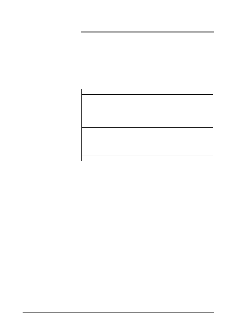
Table 3.14.1
Order of Current Consumption
At initial setting with the CPU in operation mode, the CPU is
ready with OSC3 clock (CLKCHG = 0, in high-speed mode),
the ceramic (CR) oscillation circuit is ON (OSCC = 1), the
REM circuit is ON (REMC = 1), the timer is OFF (TMRUN =
0), the SVD circuit is OFF (SVDON = 0), and the AMP circuit
is OFF (OPON = 0).
It should be noted that various factors affecting current
consumption. For example, a system in which a resistor is
connected to the VADJ pin to control the LCD power (VL1)
differ from a system in which the VADJ pin is shorted to VL1.
Also, characteristics of the LCD panel used will produce a
difference in power consumption to the order of several
micro-amperes.
CPU
CPU operating
frequency
Ceramic (CR)
oscillation
circuit
REM circuit
Timer
SVD circuit
AMP circuit
HALT instruction
CLKCHG
OSCC
REMC
TMRUN
SVDON
OPON
See section 5
"ELECTRICAL CHARACTERISTICS"
Several tens A
Several A (in OSC3 mode)
Several hundreds nA
(OSC3 not used, option used)
Several hundreds nA
Several tens A
Circuit block
Control register
Order of current consumption
相關PDF資料 |
PDF描述 |
|---|---|
| MQ80C32E-12 | 8-BIT, 12 MHz, MICROCONTROLLER, CQFP44 |
| MQ80C52CXXX-16:D | 8-BIT, MROM, 16 MHz, MICROCONTROLLER, CQFP44 |
| MR83C154CXXX-36/883 | 8-BIT, MROM, 36 MHz, MICROCONTROLLER, CQCC44 |
| MR80C52TXXX-36SHXXX:D | 8-BIT, MROM, 36 MHz, MICROCONTROLLER, CQCC44 |
| MR80C52TXXX-36SHXXX:D | 8-BIT, MROM, 36 MHz, MICROCONTROLLER, CQCC44 |
相關代理商/技術參數(shù) |
參數(shù)描述 |
|---|---|
| MQ82370-20 | 制造商:Rochester Electronics LLC 功能描述:- Bulk |
| MQ8238020 | 制造商:Intel 功能描述:CONTROLLER: OTHER |
| MQ82380-20 | 制造商:Rochester Electronics LLC 功能描述:- Bulk |
| MQ82380-20/R | 制造商:Rochester Electronics LLC 功能描述: |
| MQ82592 | 制造商:Rochester Electronics LLC 功能描述:- Bulk |
發(fā)布緊急采購,3分鐘左右您將得到回復。