- 您現(xiàn)在的位置:買賣IC網(wǎng) > PDF目錄383634 > MPS8599G (ON SEMICONDUCTOR) Amplifier Transistors Voltage and Current are Negative for PNP Transistors PDF資料下載
參數(shù)資料
| 型號(hào): | MPS8599G |
| 廠商: | ON SEMICONDUCTOR |
| 元件分類: | 功率晶體管 |
| 英文描述: | Amplifier Transistors Voltage and Current are Negative for PNP Transistors |
| 中文描述: | 500 mA, 80 V, PNP, Si, SMALL SIGNAL TRANSISTOR, TO-92 |
| 封裝: | LEAD FREE, CASE 29-11, TO-226, 3 PIN |
| 文件頁數(shù): | 1/7頁 |
| 文件大小: | 90K |
| 代理商: | MPS8599G |
Semiconductor Components Industries, LLC, 2006
January, 2006 Rev. 5
1
Publication Order Number:
MPS8098/D
(NPN) MPS8098, MPS8099*,
(PNP) MPS8598, MPS8599*
*Preferred Devices
Amplifier Transistors
Voltage and Current are Negative
for PNP Transistors
Features
PbFree Packages are Available*
MAXIMUM RATINGS
Rating
Symbol
Value
Unit
CollectorEmitter Voltage
MPS8098, MPS8598
MPS8099, MPS8599
V
CEO
60
80
Vdc
CollectorBase Voltage
MPS8098, MPS8598
MPS8099, MPS8599
V
CBO
60
80
Vdc
EmitterBase Voltage
V
EBO
4.0
Vdc
Collector Current Continuous
I
C
500
mAdc
Total Device Dissipation @ T
A
= 25
°
C
Derate above 25
°
C
P
D
625
5.0
mW
mW/
°
C
Total Device Dissipation @ T
C
= 25
°
C
Derate above 25
°
C
P
D
1.5
12
W
mW/
°
C
Operating and Storage Junction
Temperature Range
T
J
, T
stg
55 to +150
°
C
THERMAL CHARACTERISTICS
Characteristic
Symbol
Max
Unit
Thermal Resistance, JunctiontoAmbient
(Note 1)
R
JA
200
°
C/W
Thermal Resistance, JunctiontoCase
R
JC
83.3
°
C/W
Maximum ratings are those values beyond which device damage can occur.
Maximum ratings applied to the device are individual stress limit values (not
normal operating conditions) and are not valid simultaneously. If these limits are
exceeded, device functional operation is not implied, damage may occur and
reliability may be affected.
1. R
JA
is measured with the device soldered into a typical printed circuit board.
*For additional information on our PbFree strategy and soldering details, please
download the ON Semiconductor Soldering and Mounting Techniques
Reference Manual, SOLDERRM/D.
Preferred
devices are recommended choices for future use
and best overall value.
http://onsemi.com
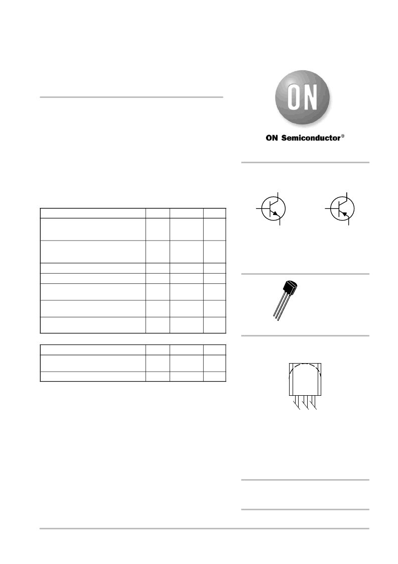
COLLECTOR
3
2
BASE
1
EMITTER
STYLE 1
MPS8098,
MPS8099
NPN
COLLECTOR
3
2
BASE
1
EMITTER
STYLE 1
MPS8598,
MPS8599
PNP
See detailed ordering and shipping information in the package
dimensions section on page 6 of this data sheet.
ORDERING INFORMATION
MPS8x9y = Device Code
x = 0 or 5
y = 8 or 9
= Assembly Location
= Year
= Work Week
= PbFree Package
A
Y
WW
(Note: Microdot may be in either location)
TO92
CASE 2911
STYLE 1
1
23
MARKING DIAGRAM
MPS
8x9y
AYWW
相關(guān)PDF資料 |
PDF描述 |
|---|---|
| MPSA06 | NPN General Purpose Transistor(通用NPN晶體管) |
| MPSA12G | Darlington Transistors NPN Silicon |
| MPSA12RLRA | Darlington Transistors NPN Silicon |
| MPSA12RLRAG | Darlington Transistors NPN Silicon |
| MPSA12RLRP | Darlington Transistors NPN Silicon |
相關(guān)代理商/技術(shù)參數(shù) |
參數(shù)描述 |
|---|---|
| MPS8599RLRA | 功能描述:兩極晶體管 - BJT 500mA 80V PNP RoHS:否 制造商:STMicroelectronics 配置: 晶體管極性:PNP 集電極—基極電壓 VCBO: 集電極—發(fā)射極最大電壓 VCEO:- 40 V 發(fā)射極 - 基極電壓 VEBO:- 6 V 集電極—射極飽和電壓: 最大直流電集電極電流: 增益帶寬產(chǎn)品fT: 直流集電極/Base Gain hfe Min:100 A 最大工作溫度: 安裝風(fēng)格:SMD/SMT 封裝 / 箱體:PowerFLAT 2 x 2 |
| MPS8599RLRAG | 功能描述:兩極晶體管 - BJT 500mA 80V PNP RoHS:否 制造商:STMicroelectronics 配置: 晶體管極性:PNP 集電極—基極電壓 VCBO: 集電極—發(fā)射極最大電壓 VCEO:- 40 V 發(fā)射極 - 基極電壓 VEBO:- 6 V 集電極—射極飽和電壓: 最大直流電集電極電流: 增益帶寬產(chǎn)品fT: 直流集電極/Base Gain hfe Min:100 A 最大工作溫度: 安裝風(fēng)格:SMD/SMT 封裝 / 箱體:PowerFLAT 2 x 2 |
| MPS8599RLRM | 制造商:ONSEMI 制造商全稱:ON Semiconductor 功能描述:Amplifier Transistors Voltage and Current are Negative for PNP Transistors |
| MPS8599RLRMG | 功能描述:兩極晶體管 - BJT 500mA 80V PNP RoHS:否 制造商:STMicroelectronics 配置: 晶體管極性:PNP 集電極—基極電壓 VCBO: 集電極—發(fā)射極最大電壓 VCEO:- 40 V 發(fā)射極 - 基極電壓 VEBO:- 6 V 集電極—射極飽和電壓: 最大直流電集電極電流: 增益帶寬產(chǎn)品fT: 直流集電極/Base Gain hfe Min:100 A 最大工作溫度: 安裝風(fēng)格:SMD/SMT 封裝 / 箱體:PowerFLAT 2 x 2 |
| MPS88-1000 | 功能描述:以太網(wǎng)和電信連接器 8P8C SHIELDED STRANDED FLAT RoHS:否 制造商:Pulse 產(chǎn)品:Modular Jacks 性能類別: USOC 代碼:RJ45 位置/觸點(diǎn)數(shù)量: 安裝風(fēng)格:Through Hole 端口數(shù)量:1 x 1 型式:Female 屏蔽: 電流額定值: 電壓額定值: 觸點(diǎn)電鍍: 外殼材料:Thermoplastic IP 等級(jí): |
發(fā)布緊急采購,3分鐘左右您將得到回復(fù)。