- 您現(xiàn)在的位置:買賣IC網(wǎng) > PDF目錄45375 > MPC9992ACR2 (FREESCALE SEMICONDUCTOR INC) 400 MHz, OTHER CLOCK GENERATOR, PQFP32 PDF資料下載
參數(shù)資料
| 型號: | MPC9992ACR2 |
| 廠商: | FREESCALE SEMICONDUCTOR INC |
| 元件分類: | 時鐘產(chǎn)生/分配 |
| 英文描述: | 400 MHz, OTHER CLOCK GENERATOR, PQFP32 |
| 封裝: | 7 X 7 MM, 1.40 MM HEIGHT, LEAD FREE, MS-026BBA, LQFP-32 |
| 文件頁數(shù): | 9/12頁 |
| 文件大小: | 313K |
| 代理商: | MPC9992ACR2 |
Advanced Clock Drivers Device Data
6
Freescale Semiconductor
MPC9992
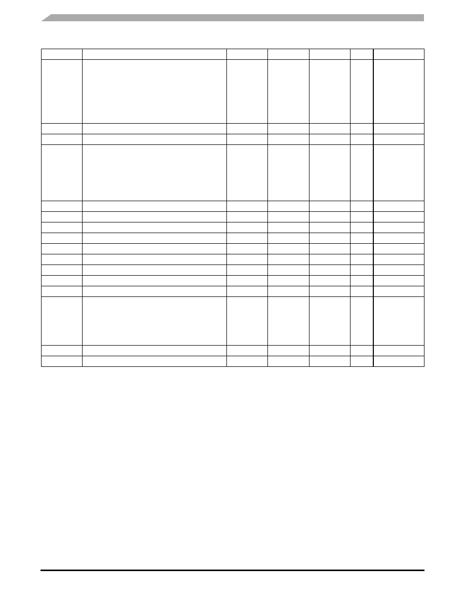
Table 7. AC Characteristics (VCC = 3.3 V ± 5%, GND = 0 V, TA = 0°C to +70°C)(1)
1. AC characteristics apply for parallel output termination of 50
to VTT.
Symbol
Characteristics
Min
Typ
Max
Unit
Condition
fref
Input Reference Frequency
÷32 feedback
÷48 feedback
÷64 feedback
÷80 feedback
÷96 feedback
÷160 feedback
Input Reference Frequency in PLL Bypass Mode(2)
2. In bypass mode, the MPC9992 divides the input reference clock.
25.0
16.67
12.5
10.0
8.33
5.0
50.0
33.3
25.0
20.0
16.67
10.0
400
MHz
PLL locked
PLL bypass
fXTAL
Crystal Interface Frequency Range(3)
3. The crystal frequency range must both meet the interface frequency range and VCO lock range divided by the feedback divider ratio:
fXTAL(min, max) = fVCO(min, max) ÷ (M VCO_SEL) and 10 MHz ≤ fXTAL ≤ 20 MHz.
10
20
MHz
fVCO
VCO Frequency Range(4)
4. The input reference frequency must match the VCO lock range divided by the total feedback divider ratio: fref = fVCO ÷ (M VCO_SEL)
800
1600
MHz
fMAX
Output Frequency
÷4 output
÷8 output
÷12 output
÷16 output
÷20 output
÷24 output
÷48 output
200.0
100.0
66.6
50.0
40.0
33.3
16.6
400.0
200.0
133.3
100.0
80.0
66.6
33.3
MHz
PLL locked
VPP
Differential Input Voltage(5) (peak-to-peak)
5. VPP is the minimum differential input voltage swing required to maintain AC characteristics.
0.3
1.3
V
VCMR
Differential Input Crosspoint Voltage(6)
(PCLK)
6. VCMR (AC) is the crosspoint of the differential input signal. Normal AC operation is obtained when the crosspoint is within the VCMR (AC)
range and the input swing lies within the VPP (AC) specification.
1.2
VCC–0.3
V
VO(P-P)
Differential Output Voltage (peak-to-peak)
(PCLK)
0.6
0.8
V
tPW,MIN
Input Reference Pulse Width(7)
7. Calculation of reference duty cycle limits: DCREF,MIN = tPW,MIN fREF 100% and DCREF,MAX = 100% – DCREF, MIN. E.g. at fREF = 50 MHz
the input duty cycle range is 10% < DC < 90%.
2.0
ns
tsk(O)
Output-to-Output Skew
100
ps
DC
Output Duty Cycle(8)
8. Output duty cycle for QAx and QBx outputs. The pulse width for the QSYNC output is equal to one QAx output period tQA ± 5%.
48
50
52
%
tJIT(CC)
Cycle-to-Cycle Jitter(9)
9. Jitter data is valid fref = 25 MHz.
30
79
ps
tJIT(PER)
Period Jitter(9)
43
106
ps
tJIT()
I/O Phase Jitter(9)
RMS (1
σ)(10)
10. See application section for a jitter calculation for other confidence factors than 1
σ.
86
212
ps
BW
PLL Closed Loop Bandwidth(11)
÷32 feedback
÷48 feedback
÷64 feedback
÷80 feedback
÷96 feedback
÷160 feedback
11. –3 dB point of PLL transfer characteristics.
0.60-1.5
0.40-1.2
0.30-1.0
0.30-0.8
0.20-0.7
0.15-0.4
MHz
tLOCK
Maximum PLL Lock Time
10
ms
tr, tf
Output Rise/Fall Time
0.05
1.0
ns
20% to 80%
相關(guān)PDF資料 |
PDF描述 |
|---|---|
| MPC9992AC | 400 MHz, OTHER CLOCK GENERATOR, PQFP32 |
| MPD703226GC(A)-8EU | RISC MICROCONTROLLER, PQFP100 |
| MPD703223GC(A)-8EU | RISC MICROCONTROLLER, PQFP100 |
| MPD703224GC(A)-8EU | RISC MICROCONTROLLER, PQFP100 |
| MPD78C12AGQA-XXX-36 | 8-BIT, MROM, 15 MHz, MICROCONTROLLER, PZIP64 |
相關(guān)代理商/技術(shù)參數(shù) |
參數(shù)描述 |
|---|---|
| MPC9992FA | 功能描述:鎖相環(huán) - PLL 2.5 3.3V 400MHz Clock Generator RoHS:否 制造商:Silicon Labs 類型:PLL Clock Multiplier 電路數(shù)量:1 最大輸入頻率:710 MHz 最小輸入頻率:0.002 MHz 輸出頻率范圍:0.002 MHz to 808 MHz 電源電壓-最大:3.63 V 電源電壓-最小:1.71 V 最大工作溫度:+ 85 C 最小工作溫度:- 40 C 封裝 / 箱體:QFN-36 封裝:Tray |
| MPC9992FAR2 | 制造商:Integrated Device Technology Inc 功能描述:PLL Clock Driver Single 32-Pin LQFP T/R |
| MPC9993 | 制造商:MOTOROLA 制造商全稱:Motorola, Inc 功能描述:INTELLIGENT DYNAMIC CLOCK SWITCH (IDCS)PLL CLOCK DRIVER |
| MPC9993AC | 功能描述:時鐘驅(qū)動器及分配 RoHS:否 制造商:Micrel 乘法/除法因子:1:4 輸出類型:Differential 最大輸出頻率:4.2 GHz 電源電壓-最大: 電源電壓-最小:5 V 最大工作溫度:+ 85 C 封裝 / 箱體:SOIC-8 封裝:Reel |
| MPC9993ACR2 | 功能描述:時鐘驅(qū)動器及分配 RoHS:否 制造商:Micrel 乘法/除法因子:1:4 輸出類型:Differential 最大輸出頻率:4.2 GHz 電源電壓-最大: 電源電壓-最小:5 V 最大工作溫度:+ 85 C 封裝 / 箱體:SOIC-8 封裝:Reel |
發(fā)布緊急采購,3分鐘左右您將得到回復(fù)。