- 您現(xiàn)在的位置:買賣IC網(wǎng) > PDF目錄26839 > MPC9658FA (MOTOROLA INC) PLL BASED CLOCK DRIVER, 10 TRUE OUTPUT(S), 0 INVERTED OUTPUT(S), PQFP32 PDF資料下載
參數(shù)資料
| 型號: | MPC9658FA |
| 廠商: | MOTOROLA INC |
| 元件分類: | 時鐘及定時 |
| 英文描述: | PLL BASED CLOCK DRIVER, 10 TRUE OUTPUT(S), 0 INVERTED OUTPUT(S), PQFP32 |
| 封裝: | 7 X 7 MM, LQFP-32 |
| 文件頁數(shù): | 8/9頁 |
| 文件大?。?/td> | 144K |
| 代理商: | MPC9658FA |
5
MPC9658
MOTOROLA ADVANCED CLOCK DRIVERS DEVICE DATA
525
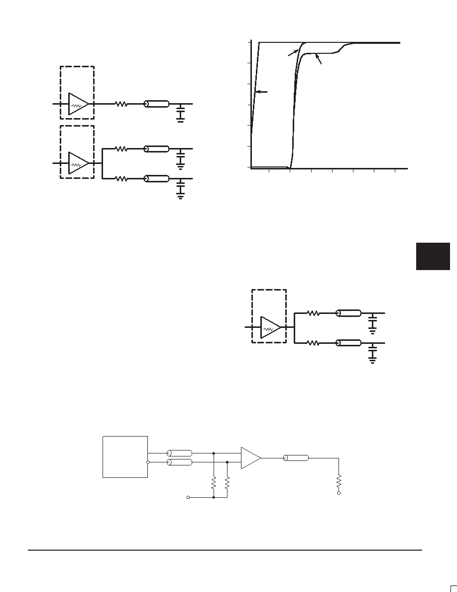
parallel. When taken to its extreme the fanout of the MPC9658
clock driver is effectively doubled due to its capability to drive
multiple lines.
Figure 6. Single versus Dual Transmission Lines
14
IN
MPC9658
OUTPUT
BUFFER
RS = 36
ZO = 50
OutA
14
IN
MPC9658
OUTPUT
BUFFER
RS = 36
ZO = 50
OutB0
RS = 36
ZO = 50
OutB1
The waveform plots in Figure 7 “Single versus Dual Line
Termination Waveforms” show the simulation results of an out-
put driving a single line versus two lines. In both cases the
drive capability of the MPC9658 output buffer is more than suf-
ficient to drive 50
transmission lines on the incident edge.
Note from the delay measurements in the simulations a delta
of only 43ps exists between the two differently loaded outputs.
This suggests that the dual line driving need not be used exclu-
sively to maintain the tight output-to-output skew of the
MPC9658. The output waveform in Figure 7 “Single versus
Dual Line Termination Waveforms” shows a step in the wave-
form, this step is caused by the impedance mismatch seen
looking into the driver. The parallel combination of the 36
se-
ries resistor plus the output impedance does not match the
parallel combination of the line impedances. The voltage wave
launched down the two lines will equal:
VL = VS ( Z0 ÷ (RS+R0 +Z0))
Z0 = 50 || 50
RS = 36 || 36
R0 = 14
VL = 3.0 ( 25 ÷ (18+14+25)
= 1.31V
At the load end the voltage will double, due to the near unity
reflection coefficient, to 2.6V. It will then increment towards the
quiescent 3.0V in steps separated by one round trip delay (in
this case 4.0ns).
Figure 7. Single versus Dual Waveforms
TIME (nS)
VOL
TAGE
(V)
3.0
2.5
2.0
1.5
1.0
0.5
0
2
4
6
8
10
12
14
OutB
tD = 3.9386
OutA
tD = 3.8956
In
Since this step is well above the threshold region it will not
cause any false clock triggering, however designers may be
uncomfortable with unwanted reflections on the line. To better
match the impedances when driving multiple lines the situation
in Figure 8 “Optimized Dual Line Termination” should be used.
In this case the series terminating resistors are reduced such
that when the parallel combination is added to the output buffer
impedance the line impedance is perfectly matched.
Figure 8. Optimized Dual Line Termination
14
MPC9658
OUTPUT
BUFFER
RS = 22
ZO = 50
RS = 22
ZO = 50
14
+ 22 k 22 = 50 k 50
25
= 25
Figure 9. PCLK MPC9658 AC test reference
Differential
Pulse Generator
Z = 50 W
RT = 50
ZO = 50
RT = 50
ZO = 50
MPC9658 DUT
VTT
相關(guān)PDF資料 |
PDF描述 |
|---|---|
| MPC96877VKR2 | 96877 SERIES, PLL BASED CLOCK DRIVER, 10 TRUE OUTPUT(S), 0 INVERTED OUTPUT(S), PBGA52 |
| MPC974FAR2 | 974 SERIES, PLL BASED CLOCK DRIVER, 14 TRUE OUTPUT(S), 0 INVERTED OUTPUT(S), PQFP52 |
| MPC9774FA | 9774 SERIES, PLL BASED CLOCK DRIVER, 14 TRUE OUTPUT(S), 0 INVERTED OUTPUT(S), PQFP52 |
| MPC9774AE | 9774 SERIES, PLL BASED CLOCK DRIVER, 14 TRUE OUTPUT(S), 0 INVERTED OUTPUT(S), PQFP52 |
| MPC97H73FAR2 | PLL BASED CLOCK DRIVER, 13 TRUE OUTPUT(S), 0 INVERTED OUTPUT(S), PQFP52 |
相關(guān)代理商/技術(shù)參數(shù) |
參數(shù)描述 |
|---|---|
| MPC9658FAR2 | 制造商:Integrated Device Technology Inc 功能描述:PLL Clock Driver Single 32-Pin LQFP T/R 制造商:Integrated Device Technology Inc 功能描述:MPC9658FAR2 - Tape and Reel |
| MPC96877VK | 功能描述:時鐘發(fā)生器及支持產(chǎn)品 DDR2 PLL RoHS:否 制造商:Silicon Labs 類型:Clock Generators 最大輸入頻率:14.318 MHz 最大輸出頻率:166 MHz 輸出端數(shù)量:16 占空比 - 最大:55 % 工作電源電壓:3.3 V 工作電源電流:1 mA 最大工作溫度:+ 85 C 安裝風(fēng)格:SMD/SMT 封裝 / 箱體:QFN-56 |
| MPC96877VKR2 | 功能描述:時鐘發(fā)生器及支持產(chǎn)品 DDR2 PLL RoHS:否 制造商:Silicon Labs 類型:Clock Generators 最大輸入頻率:14.318 MHz 最大輸出頻率:166 MHz 輸出端數(shù)量:16 占空比 - 最大:55 % 工作電源電壓:3.3 V 工作電源電流:1 mA 最大工作溫度:+ 85 C 安裝風(fēng)格:SMD/SMT 封裝 / 箱體:QFN-56 |
| MPC970 | 制造商:MOTOROLA 制造商全稱:Motorola, Inc 功能描述:LOW VOLTAGE PLL CLOCK DRIVER |
| MPC972 | 制造商:Motorola Inc 功能描述: |
發(fā)布緊急采購,3分鐘左右您將得到回復(fù)。