- 您現在的位置:買賣IC網 > PDF目錄69037 > MPC930FA (INTEGRATED DEVICE TECHNOLOGY INC) 140 MHz, PROC SPECIFIC CLOCK GENERATOR, PQFP32 PDF資料下載
參數資料
| 型號: | MPC930FA |
| 廠商: | INTEGRATED DEVICE TECHNOLOGY INC |
| 元件分類: | 時鐘產生/分配 |
| 英文描述: | 140 MHz, PROC SPECIFIC CLOCK GENERATOR, PQFP32 |
| 封裝: | TQFP-32 |
| 文件頁數: | 3/14頁 |
| 文件大小: | 544K |
| 代理商: | MPC930FA |
MPC930 MPC931
ECLinPS and ECLinPS Lite
DL140 — Rev 3
11
MOTOROLA
Figure 15. PLL Block Diagram
fref
Phase
Detector
Qn
VCO
LPF
÷P
÷N
÷m
N fref +
fQn N P
m
fref +
fVCO
m
,fVCO + fQnNP
m = 8
P = 1 (Power_Dn=‘0’), 2 (Power_Dn=‘1’)
For the MPC930 clock driver, the following will provide an
example of how to determine the crystal frequency required
for a given design.
Given:
Qa
= 66.6MHz
Qb
= 33.3MHz
Qc
= 22.2MHz
Power_Dn = ‘0’
fref +
fQn N P
m
From Table 4
fQc = VCO/6 then N = 6
From Figure 15
m = 8 and P = 1
fref +
22.22 6 1
8
+ 16.66MHz
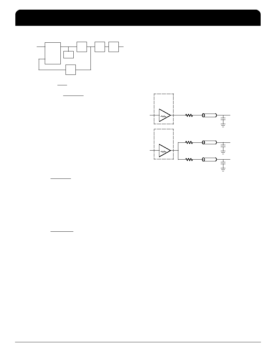
Driving Transmission Lines
The MPC930/931 clock driver was designed to drive high
speed signals in a terminated transmission line environment.
To provide the optimum flexibility to the user the output
drivers were designed to exhibit the lowest impedance
possible. With an output impedance of less than 10
the
drivers can drive either parallel or series terminated
transmission lines. For more information on transmission
lines the reader is referred to application note AN1091 in the
Timing Solutions brochure (BR1333/D).
In most high performance clock networks point–to–point
distribution of signals is the method of choice. In a
point–to–point scheme either series terminated or parallel
terminated transmission lines can be used. The parallel
technique terminates the signal at the end of the line with a
50
resistance to VCC/2. This technique draws a fairly high
level of DC current and thus only a single terminated line can
be driven by each output of the MPC930/931 clock driver. For
the series terminated case however there is no DC current
draw, thus the outputs can drive multiple series terminated
lines. Figure 16 illustrates an output driving a single series
terminated line vs two series terminated lines in parallel.
When taken to its extreme the fanout of the MPC930/931
clock driver is effectively doubled due to its capability to drive
multiple lines.
Figure 16. Single versus Dual Transmission Lines
7
IN
MPC930/931
OUTPUT
BUFFER
RS = 43
ZO = 50
OutA
7
IN
MPC930/931
OUTPUT
BUFFER
RS = 43
ZO = 50
OutB0
RS = 43
ZO = 50
OutB1
The waveform plots of Figure 17 show the simulation
results of an output driving a single line vs two lines. In both
cases the drive capability of the MPC930/931 output buffers
is more than sufficient to drive 50
transmission lines on the
incident edge. Note from the delay measurements in the
simulations a delta of only 43ps exists between the two
differently loaded outputs. This suggests that the dual line
driving need not be used exclusively to maintain the tight
output–to–output skew of the MPC930/931. The output
waveform in Figure 17 shows a step in the waveform, this
step is caused by the impedance mismatch seen looking into
the driver. The parallel combination of the 43
series resistor
plus the output impedance does not match the parallel
combination of the line impedances. The voltage wave
launched down the two lines will equal:
VL = VS ( Zo / (Rs + Ro +Zo))
Zo = 50
|| 50
Rs = 43
|| 43
Ro = 7
VL = 3.0 (25 / (21.5 + 7 + 25) = 3.0 (25 / 53.5)
= 1.40V
At the load end the voltage will double, due to the near
unity reflection coefficient, to 2.8V. It will then increment
towards the quiescent 3.0V in steps separated by one round
trip delay (in this case 4.0ns).
F
re
e
sc
a
le
S
e
m
ic
o
n
d
u
c
to
r,
I
Freescale Semiconductor, Inc.
For More Information On This Product,
Go to: www.freescale.com
n
c
..
.
MPC930 MPC931
Low Voltage PLL Clock Driver
NETCOM
IDT Low Voltage PLL Clock Driver
Freescale Timing Solutions Organization has been acquired by Integrated Device Technology, Inc
MPC930 MPC931
11
相關PDF資料 |
PDF描述 |
|---|---|
| MPC930FA | 140 MHz, PROC SPECIFIC CLOCK GENERATOR, PQFP32 |
| MPC972FA | 125 MHz, PROC SPECIFIC CLOCK GENERATOR, PQFP52 |
| MPC9850VF | 500 MHz, PROC SPECIFIC CLOCK GENERATOR, PBGA100 |
| MPC9850VMR2 | 500 MHz, PROC SPECIFIC CLOCK GENERATOR, PBGA100 |
| MPC9850VMR2 | 500 MHz, PROC SPECIFIC CLOCK GENERATOR, PBGA100 |
相關代理商/技術參數 |
參數描述 |
|---|---|
| MPC931 | 制造商:Motorola Inc 功能描述: |
| MPC9315 | 制造商:MOTOROLA 制造商全稱:Motorola, Inc 功能描述:2.5V and 3.3V CMOS PLL Clock Generator and Driver |
| MPC9315AC | 功能描述:鎖相環(huán) - PLL 2.5 3.3V 160MHz Clock Generator RoHS:否 制造商:Silicon Labs 類型:PLL Clock Multiplier 電路數量:1 最大輸入頻率:710 MHz 最小輸入頻率:0.002 MHz 輸出頻率范圍:0.002 MHz to 808 MHz 電源電壓-最大:3.63 V 電源電壓-最小:1.71 V 最大工作溫度:+ 85 C 最小工作溫度:- 40 C 封裝 / 箱體:QFN-36 封裝:Tray |
| MPC9315ACR2 | 功能描述:時鐘發(fā)生器及支持產品 FSL 1-8 LVCMOS PLL Clock Generator RoHS:否 制造商:Silicon Labs 類型:Clock Generators 最大輸入頻率:14.318 MHz 最大輸出頻率:166 MHz 輸出端數量:16 占空比 - 最大:55 % 工作電源電壓:3.3 V 工作電源電流:1 mA 最大工作溫度:+ 85 C 安裝風格:SMD/SMT 封裝 / 箱體:QFN-56 |
| MPC9315FA | 功能描述:鎖相環(huán) - PLL 2.5 3.3V 160MHz Clock Generator RoHS:否 制造商:Silicon Labs 類型:PLL Clock Multiplier 電路數量:1 最大輸入頻率:710 MHz 最小輸入頻率:0.002 MHz 輸出頻率范圍:0.002 MHz to 808 MHz 電源電壓-最大:3.63 V 電源電壓-最小:1.71 V 最大工作溫度:+ 85 C 最小工作溫度:- 40 C 封裝 / 箱體:QFN-36 封裝:Tray |
發(fā)布緊急采購,3分鐘左右您將得到回復。