- 您現(xiàn)在的位置:買賣IC網(wǎng) > PDF目錄45366 > MPC8533EVTALJB (FREESCALE SEMICONDUCTOR INC) 32-BIT, 667 MHz, RISC PROCESSOR, PBGA783 PDF資料下載
參數(shù)資料
| 型號(hào): | MPC8533EVTALJB |
| 廠商: | FREESCALE SEMICONDUCTOR INC |
| 元件分類: | 微控制器/微處理器 |
| 英文描述: | 32-BIT, 667 MHz, RISC PROCESSOR, PBGA783 |
| 封裝: | 29 X 29 MM, 1 MM PITCH, LEAD FREE, PLASTIC, BGA-783 |
| 文件頁(yè)數(shù): | 32/116頁(yè) |
| 文件大?。?/td> | 1277K |
| 代理商: | MPC8533EVTALJB |
第1頁(yè)第2頁(yè)第3頁(yè)第4頁(yè)第5頁(yè)第6頁(yè)第7頁(yè)第8頁(yè)第9頁(yè)第10頁(yè)第11頁(yè)第12頁(yè)第13頁(yè)第14頁(yè)第15頁(yè)第16頁(yè)第17頁(yè)第18頁(yè)第19頁(yè)第20頁(yè)第21頁(yè)第22頁(yè)第23頁(yè)第24頁(yè)第25頁(yè)第26頁(yè)第27頁(yè)第28頁(yè)第29頁(yè)第30頁(yè)第31頁(yè)當(dāng)前第32頁(yè)第33頁(yè)第34頁(yè)第35頁(yè)第36頁(yè)第37頁(yè)第38頁(yè)第39頁(yè)第40頁(yè)第41頁(yè)第42頁(yè)第43頁(yè)第44頁(yè)第45頁(yè)第46頁(yè)第47頁(yè)第48頁(yè)第49頁(yè)第50頁(yè)第51頁(yè)第52頁(yè)第53頁(yè)第54頁(yè)第55頁(yè)第56頁(yè)第57頁(yè)第58頁(yè)第59頁(yè)第60頁(yè)第61頁(yè)第62頁(yè)第63頁(yè)第64頁(yè)第65頁(yè)第66頁(yè)第67頁(yè)第68頁(yè)第69頁(yè)第70頁(yè)第71頁(yè)第72頁(yè)第73頁(yè)第74頁(yè)第75頁(yè)第76頁(yè)第77頁(yè)第78頁(yè)第79頁(yè)第80頁(yè)第81頁(yè)第82頁(yè)第83頁(yè)第84頁(yè)第85頁(yè)第86頁(yè)第87頁(yè)第88頁(yè)第89頁(yè)第90頁(yè)第91頁(yè)第92頁(yè)第93頁(yè)第94頁(yè)第95頁(yè)第96頁(yè)第97頁(yè)第98頁(yè)第99頁(yè)第100頁(yè)第101頁(yè)第102頁(yè)第103頁(yè)第104頁(yè)第105頁(yè)第106頁(yè)第107頁(yè)第108頁(yè)第109頁(yè)第110頁(yè)第111頁(yè)第112頁(yè)第113頁(yè)第114頁(yè)第115頁(yè)第116頁(yè)
MPC8533E PowerQUICC III Integrated Processor Hardware Specifications, Rev. 2
22
Freescale Semiconductor
DDR and DDR2 SDRAM
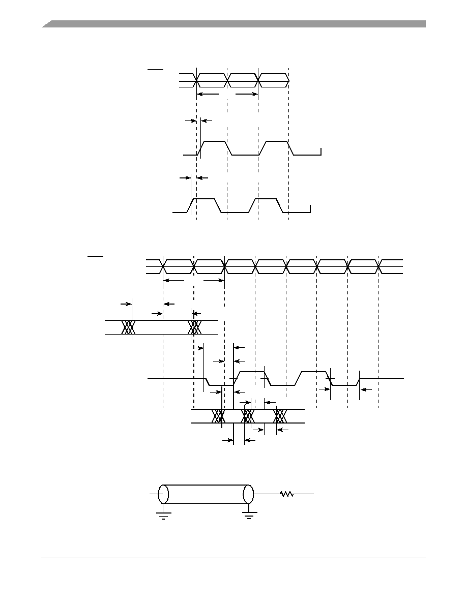
Figure 4. Timing Diagram for tDDKHMH
Figure 5 shows the DDR SDRAM output timing diagram.
Figure 5. DDR and DDR2 SDRAM Output Timing Diagram
Figure 6 provides the AC test load for the DDR bus.
Figure 6. DDR AC Test Load
MDQS
MCK[n]
tMCK
MDQS
tDDKHMH(max) = 0.6 ns
tDDKHMH(min) = –0.6 ns
ADDR/CMD
tDDKHAS, tDDKHCS
tDDKLDS
tDDKHDS
MDQ[x]
MDQS[n]
MCK
tMCK
tDDKLDX
tDDKHDX
D1
D0
tDDKHAX, tDDKHCX
Write A0
NOOP
tDDKHME
tDDKHMP
tDDKHMH
Output
Z0 = 50 Ω
GVDD/2
RL = 50 Ω
相關(guān)PDF資料 |
PDF描述 |
|---|---|
| MPC8533VTARFB | 32-BIT, 1067 MHz, RISC PROCESSOR, PBGA783 |
| MPC8533VTANGB | 32-BIT, 800 MHz, RISC PROCESSOR, PBGA783 |
| MPC8533VTAQGB | 32-BIT, 1000 MHz, RISC PROCESSOR, PBGA783 |
| MPC8533EVTARJB | 32-BIT, 1067 MHz, RISC PROCESSOR, PBGA783 |
| MPC8533VTALJB | 32-BIT, 667 MHz, RISC PROCESSOR, PBGA783 |
相關(guān)代理商/技術(shù)參數(shù) |
參數(shù)描述 |
|---|---|
| MPC8533EVTANG | 功能描述:微處理器 - MPU PQ38K 8533E RoHS:否 制造商:Atmel 處理器系列:SAMA5D31 核心:ARM Cortex A5 數(shù)據(jù)總線寬度:32 bit 最大時(shí)鐘頻率:536 MHz 程序存儲(chǔ)器大小:32 KB 數(shù)據(jù) RAM 大小:128 KB 接口類型:CAN, Ethernet, LIN, SPI,TWI, UART, USB 工作電源電壓:1.8 V to 3.3 V 最大工作溫度:+ 85 C 安裝風(fēng)格:SMD/SMT 封裝 / 箱體:FBGA-324 |
| MPC8533EVTANGA | 功能描述:微處理器 - MPU PQ38K 8533E RoHS:否 制造商:Atmel 處理器系列:SAMA5D31 核心:ARM Cortex A5 數(shù)據(jù)總線寬度:32 bit 最大時(shí)鐘頻率:536 MHz 程序存儲(chǔ)器大小:32 KB 數(shù)據(jù) RAM 大小:128 KB 接口類型:CAN, Ethernet, LIN, SPI,TWI, UART, USB 工作電源電壓:1.8 V to 3.3 V 最大工作溫度:+ 85 C 安裝風(fēng)格:SMD/SMT 封裝 / 箱體:FBGA-324 |
| MPC8533EVTAQG | 功能描述:微處理器 - MPU PQ38K 8533E RoHS:否 制造商:Atmel 處理器系列:SAMA5D31 核心:ARM Cortex A5 數(shù)據(jù)總線寬度:32 bit 最大時(shí)鐘頻率:536 MHz 程序存儲(chǔ)器大小:32 KB 數(shù)據(jù) RAM 大小:128 KB 接口類型:CAN, Ethernet, LIN, SPI,TWI, UART, USB 工作電源電壓:1.8 V to 3.3 V 最大工作溫度:+ 85 C 安裝風(fēng)格:SMD/SMT 封裝 / 箱體:FBGA-324 |
| MPC8533EVTAQGA | 功能描述:微處理器 - MPU PQ38K 8533E RoHS:否 制造商:Atmel 處理器系列:SAMA5D31 核心:ARM Cortex A5 數(shù)據(jù)總線寬度:32 bit 最大時(shí)鐘頻率:536 MHz 程序存儲(chǔ)器大小:32 KB 數(shù)據(jù) RAM 大小:128 KB 接口類型:CAN, Ethernet, LIN, SPI,TWI, UART, USB 工作電源電壓:1.8 V to 3.3 V 最大工作溫度:+ 85 C 安裝風(fēng)格:SMD/SMT 封裝 / 箱體:FBGA-324 |
| MPC8533EVTARJ | 功能描述:微處理器 - MPU PQ38K 8533E RoHS:否 制造商:Atmel 處理器系列:SAMA5D31 核心:ARM Cortex A5 數(shù)據(jù)總線寬度:32 bit 最大時(shí)鐘頻率:536 MHz 程序存儲(chǔ)器大小:32 KB 數(shù)據(jù) RAM 大小:128 KB 接口類型:CAN, Ethernet, LIN, SPI,TWI, UART, USB 工作電源電壓:1.8 V to 3.3 V 最大工作溫度:+ 85 C 安裝風(fēng)格:SMD/SMT 封裝 / 箱體:FBGA-324 |
發(fā)布緊急采購(gòu),3分鐘左右您將得到回復(fù)。