- 您現(xiàn)在的位置:買賣IC網(wǎng) > PDF目錄45365 > MPC8378CVRAJDA (FREESCALE SEMICONDUCTOR INC) 32-BIT, 266 MHz, MICROPROCESSOR, PBGA689 PDF資料下載
參數(shù)資料
| 型號(hào): | MPC8378CVRAJDA |
| 廠商: | FREESCALE SEMICONDUCTOR INC |
| 元件分類: | 微控制器/微處理器 |
| 英文描述: | 32-BIT, 266 MHz, MICROPROCESSOR, PBGA689 |
| 封裝: | 31 X 31 MM, 2.46 MM HEIGHT, 1 MM PITCH, LEAD FREE, PLASTIC, BGA-689 |
| 文件頁數(shù): | 82/125頁 |
| 文件大小: | 894K |
| 代理商: | MPC8378CVRAJDA |
第1頁第2頁第3頁第4頁第5頁第6頁第7頁第8頁第9頁第10頁第11頁第12頁第13頁第14頁第15頁第16頁第17頁第18頁第19頁第20頁第21頁第22頁第23頁第24頁第25頁第26頁第27頁第28頁第29頁第30頁第31頁第32頁第33頁第34頁第35頁第36頁第37頁第38頁第39頁第40頁第41頁第42頁第43頁第44頁第45頁第46頁第47頁第48頁第49頁第50頁第51頁第52頁第53頁第54頁第55頁第56頁第57頁第58頁第59頁第60頁第61頁第62頁第63頁第64頁第65頁第66頁第67頁第68頁第69頁第70頁第71頁第72頁第73頁第74頁第75頁第76頁第77頁第78頁第79頁第80頁第81頁當(dāng)前第82頁第83頁第84頁第85頁第86頁第87頁第88頁第89頁第90頁第91頁第92頁第93頁第94頁第95頁第96頁第97頁第98頁第99頁第100頁第101頁第102頁第103頁第104頁第105頁第106頁第107頁第108頁第109頁第110頁第111頁第112頁第113頁第114頁第115頁第116頁第117頁第118頁第119頁第120頁第121頁第122頁第123頁第124頁第125頁
MPC8378E PowerQUICC II Pro Processor Hardware Specifications, Rev. 5
Freescale Semiconductor
6
2
Electrical Characteristics
This section provides the AC and DC electrical specifications and thermal characteristics for the MPC8378E. The device is
currently targeted to these specifications. Some of these specifications are independent of the I/O cell, but are included for a
more complete reference. These are not purely I/O buffer design specifications.
2.1
Overall DC Electrical Characteristics
This section covers the ratings, conditions, and other characteristics.
2.1.1
Absolute Maximum Ratings
The following table provides the absolute maximum ratings.
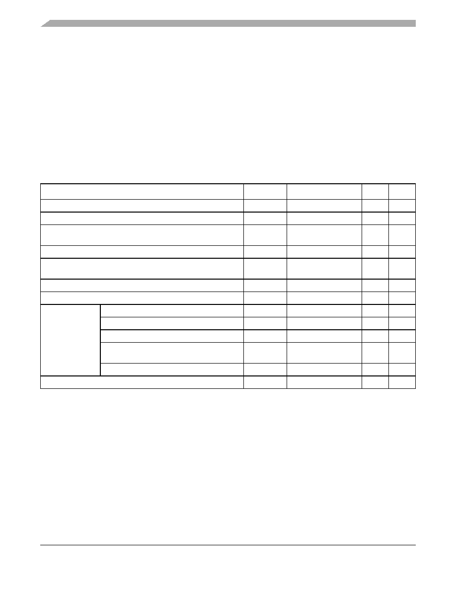
Table 2. Absolute Maximum Ratings1
Characteristic
Symbol
Max Value
Unit
Note
Core supply voltage
VDD
–0.3 to 1.1
V
—
PLL supply voltage (e300 core, eLBC, and system)
AVDD
–0.3 to 1.1
V
—
DDR1 and DDR2 DRAM I/O voltage
GVDD
–0.3 to 2.75
–0.3 to 1.98
V—
Three-speed Ethernet I/O, MII management voltage
–0.3 to 3.63
V
—
PCI, DUART, system control and power management, I2C, and JTAG
I/O voltage
OVDD
–0.3 to 3.63
V
—
Local bus
LBVDD
–0.3 to 3.63
V
—
SerDes
–0.3 to 1.1
V
Input voltage
DDR DRAM signals
MVIN
–0.3 to (GVDD + 0.3)
V
DDR DRAM reference
MVREF
–0.3 to (GVDD + 0.3)
V
Three-speed Ethernet signals
LVIN
–0.3 to (LVDD + 0.3)
V
—
PCI, DUART, CLKIN, system control and power
management, I2C, and JTAG signals
OVIN
–0.3 to (OVDD + 0.3)
V
Local Bus
LBIN
–0.3 to (LBVDD + 0.3)
V
—
Storage temperature range
TSTG
–55 to 150
C—
Notes:
1. Functional and tested operating conditions are given in Table 3. Absolute maximum ratings are stress ratings only, and
functional operation at the maximums is not guaranteed. Stresses beyond those listed may affect device reliability or cause
permanent damage to the device.
2. Caution: MVIN must not exceed GVDD by more than 0.3 V. This limit may be exceeded for a maximum of 20 ms during
power-on reset and power-down sequences.
3. Caution: OVIN must not exceed OVDD by more than 0.3 V. This limit may be exceeded for a maximum of 20 ms during
power-on reset and power-down sequences.
4. (M,O)VIN and MVREF may overshoot/undershoot to a voltage and for a maximum duration as shown in Figure 2.
5. Overshoot/undershoot by OVIN on the PCI interface does not comply to the PCI Electrical Specification for 3.3-V operation,
as shown in Figure 2.
6. L[1,2]_nVDD includes SDAVDD_0, XCOREVDD, and XPADVDD power inputs.
相關(guān)PDF資料 |
PDF描述 |
|---|---|
| MPC8378ECVRALDA | 32-BIT, 266 MHz, MICROPROCESSOR, PBGA689 |
| MPC8378VRAJDA | 32-BIT, 266 MHz, MICROPROCESSOR, PBGA689 |
| MPC8378CVRANDA | 32-BIT, 266 MHz, MICROPROCESSOR, PBGA689 |
| MPC8378EVRAGFA | 32-BIT, 333 MHz, MICROPROCESSOR, PBGA689 |
| MPC8378EVRAJFA | 32-BIT, 333 MHz, MICROPROCESSOR, PBGA689 |
相關(guān)代理商/技術(shù)參數(shù) |
參數(shù)描述 |
|---|---|
| MPC8378CVRAJF | 功能描述:微處理器 - MPU PBGA W/O ENCR RoHS:否 制造商:Atmel 處理器系列:SAMA5D31 核心:ARM Cortex A5 數(shù)據(jù)總線寬度:32 bit 最大時(shí)鐘頻率:536 MHz 程序存儲(chǔ)器大小:32 KB 數(shù)據(jù) RAM 大小:128 KB 接口類型:CAN, Ethernet, LIN, SPI,TWI, UART, USB 工作電源電壓:1.8 V to 3.3 V 最大工作溫度:+ 85 C 安裝風(fēng)格:SMD/SMT 封裝 / 箱體:FBGA-324 |
| MPC8378CVRAJFA | 制造商:FREESCALE 制造商全稱:Freescale Semiconductor, Inc 功能描述:PowerQUICC? II Pro Processor Hardware Specifications |
| MPC8378CVRAJGA | 制造商:FREESCALE 制造商全稱:Freescale Semiconductor, Inc 功能描述:PowerQUICC? II Pro Processor Hardware Specifications |
| MPC8378CVRALDA | 制造商:FREESCALE 制造商全稱:Freescale Semiconductor, Inc 功能描述:PowerQUICC? II Pro Processor Hardware Specifications |
| MPC8378CVRALFA | 制造商:FREESCALE 制造商全稱:Freescale Semiconductor, Inc 功能描述:PowerQUICC? II Pro Processor Hardware Specifications |
發(fā)布緊急采購,3分鐘左右您將得到回復(fù)。