- 您現(xiàn)在的位置:買賣IC網(wǎng) > PDF目錄45360 > MPC8313ECZQAGD (FREESCALE SEMICONDUCTOR INC) 32-BIT, 400 MHz, MICROPROCESSOR, PBGA516 PDF資料下載
參數(shù)資料
| 型號: | MPC8313ECZQAGD |
| 廠商: | FREESCALE SEMICONDUCTOR INC |
| 元件分類: | 微控制器/微處理器 |
| 英文描述: | 32-BIT, 400 MHz, MICROPROCESSOR, PBGA516 |
| 封裝: | 27 X 27 MM, 2.25 MM HEIGHT, 1 MM PITCH, TEPBGAII-516 |
| 文件頁數(shù): | 20/100頁 |
| 文件大?。?/td> | 1247K |
| 代理商: | MPC8313ECZQAGD |
第1頁第2頁第3頁第4頁第5頁第6頁第7頁第8頁第9頁第10頁第11頁第12頁第13頁第14頁第15頁第16頁第17頁第18頁第19頁當(dāng)前第20頁第21頁第22頁第23頁第24頁第25頁第26頁第27頁第28頁第29頁第30頁第31頁第32頁第33頁第34頁第35頁第36頁第37頁第38頁第39頁第40頁第41頁第42頁第43頁第44頁第45頁第46頁第47頁第48頁第49頁第50頁第51頁第52頁第53頁第54頁第55頁第56頁第57頁第58頁第59頁第60頁第61頁第62頁第63頁第64頁第65頁第66頁第67頁第68頁第69頁第70頁第71頁第72頁第73頁第74頁第75頁第76頁第77頁第78頁第79頁第80頁第81頁第82頁第83頁第84頁第85頁第86頁第87頁第88頁第89頁第90頁第91頁第92頁第93頁第94頁第95頁第96頁第97頁第98頁第99頁第100頁
MPC8313E PowerQUICC II Pro Processor Hardware Specifications, Rev. 3
26
Freescale Semiconductor
Ethernet: Three-Speed Ethernet, MII Management
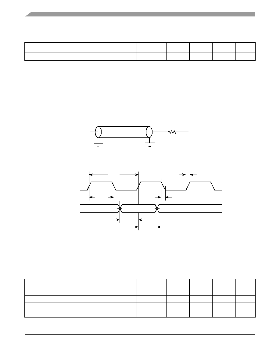
Figure 12 provides the AC test load.
Figure 12. AC Test Load
Figure 13 shows the RMII receive AC timing diagram.
Figure 13. RMII Receive AC Timing Diagram
8.2.2
RGMII and RTBI AC Timing Specifications
Table 30 presents the RGMII and RTBI AC timing specifications.
REF_CLK clock fall time VIH(max) to VIL(min)
tRMXF
1.0
—
4.0
ns
Note:
1. The symbols used for timing specifications follow the pattern of t(first three letters of functional block)(signal)(state)(reference)(state) for
inputs and t(first two letters of functional block)(reference)(state)(signal)(state) for outputs. For example, tRMRDVKH symbolizes RMII
receive timing (RMR) with respect to the time data input signals (D) reach the valid state (V) relative to the tRMX clock
reference (K) going to the high (H) state or setup time. Also, tRMRDXKL symbolizes RMII receive timing (RMR) with respect to
the time data input signals (D) went invalid (X) relative to the tRMX clock reference (K) going to the low (L) state or hold time.
Note that, in general, the clock reference symbol representation is based on three letters representing the clock of a particular
functional. For example, the subscript of tRMX represents the RMII (RM) reference (X) clock. For rise and fall times, the latter
convention is used with the appropriate letter: R (rise) or F (fall).
Table 30. RGMII and RTBI AC Timing Specifications
At recommended operating conditions with LVDDA/LVDDB of 2.5 V ± 5%.
Parameter/Condition
Symbol1
Min
Typ
Max
Unit
Data to clock output skew (at transmitter)
tSKRGT
–0.5
—
0.5
ns
Data to clock input skew (at receiver) 2
tSKRGT
1.0
—
2.8
ns
Clock cycle duration 3
tRGT
7.2
8.0
8.8
ns
Duty cycle for 1000Base-T 4, 5
tRGTH/tRGT
45
50
55
%
Table 29. RMII Receive AC Timing Specifications (continued)
At recommended operating conditions with NVDD of 3.3 V ± 0.3 V.
Parameter/Condition
Symbol1
Min
Typ
Max
Unit
Output
Z0 = 50 Ω
NVDD/2
RL = 50 Ω
REF_CLK
RXD[1:0]
tRMRDXKH
tRMX
tRMXH
tRMXR
tRMXF
CRS_DV
RX_ER
tRMRDVKH
Valid Data
相關(guān)PDF資料 |
PDF描述 |
|---|---|
| MPC8313ECVRAGDB | 32-BIT, 400 MHz, MICROPROCESSOR, PBGA516 |
| MPC8313ZQAGD | 32-BIT, 400 MHz, MICROPROCESSOR, PBGA516 |
| MPC8313ECVRAFFB | 32-BIT, 333 MHz, MICROPROCESSOR, PBGA516 |
| MPC8313EVRAGDB | 32-BIT, 400 MHz, MICROPROCESSOR, PBGA516 |
| MPC8313VRAGDB | 32-BIT, 400 MHz, MICROPROCESSOR, PBGA516 |
相關(guān)代理商/技術(shù)參數(shù) |
參數(shù)描述 |
|---|---|
| MPC8313ECZQAGDC | 功能描述:微處理器 - MPU 8313 REV2.2 PB NO EN EXT RoHS:否 制造商:Atmel 處理器系列:SAMA5D31 核心:ARM Cortex A5 數(shù)據(jù)總線寬度:32 bit 最大時鐘頻率:536 MHz 程序存儲器大小:32 KB 數(shù)據(jù) RAM 大小:128 KB 接口類型:CAN, Ethernet, LIN, SPI,TWI, UART, USB 工作電源電壓:1.8 V to 3.3 V 最大工作溫度:+ 85 C 安裝風(fēng)格:SMD/SMT 封裝 / 箱體:FBGA-324 |
| MPC8313ECZQGDD | 制造商:FREESCALE 制造商全稱:Freescale Semiconductor, Inc 功能描述:PowerQUICC? II Pro Processor Hardware Specifications |
| MPC8313ECZQGDDA | 制造商:FREESCALE 制造商全稱:Freescale Semiconductor, Inc 功能描述:PowerQUICC? II Pro Processor Hardware Specifications |
| MPC8313ECZQGDDB | 制造商:FREESCALE 制造商全稱:Freescale Semiconductor, Inc 功能描述:PowerQUICC? II Pro Processor Hardware Specifications |
| MPC8313ECZQGDF | 制造商:FREESCALE 制造商全稱:Freescale Semiconductor, Inc 功能描述:PowerQUICC? II Pro Processor Hardware Specifications |
發(fā)布緊急采購,3分鐘左右您將得到回復(fù)。