- 您現(xiàn)在的位置:買賣IC網(wǎng) > PDF目錄69036 > MPC5602PEFMLQ (FREESCALE SEMICONDUCTOR INC) MICROCONTROLLER, PQFP144 PDF資料下載
參數(shù)資料
| 型號(hào): | MPC5602PEFMLQ |
| 廠商: | FREESCALE SEMICONDUCTOR INC |
| 元件分類: | 微控制器/微處理器 |
| 英文描述: | MICROCONTROLLER, PQFP144 |
| 封裝: | 20 X 20 MM, 1.40 MM HEIGHT, 0.50 MM PITCH, LQFP-144 |
| 文件頁(yè)數(shù): | 22/72頁(yè) |
| 文件大小: | 661K |
| 代理商: | MPC5602PEFMLQ |
第1頁(yè)第2頁(yè)第3頁(yè)第4頁(yè)第5頁(yè)第6頁(yè)第7頁(yè)第8頁(yè)第9頁(yè)第10頁(yè)第11頁(yè)第12頁(yè)第13頁(yè)第14頁(yè)第15頁(yè)第16頁(yè)第17頁(yè)第18頁(yè)第19頁(yè)第20頁(yè)第21頁(yè)當(dāng)前第22頁(yè)第23頁(yè)第24頁(yè)第25頁(yè)第26頁(yè)第27頁(yè)第28頁(yè)第29頁(yè)第30頁(yè)第31頁(yè)第32頁(yè)第33頁(yè)第34頁(yè)第35頁(yè)第36頁(yè)第37頁(yè)第38頁(yè)第39頁(yè)第40頁(yè)第41頁(yè)第42頁(yè)第43頁(yè)第44頁(yè)第45頁(yè)第46頁(yè)第47頁(yè)第48頁(yè)第49頁(yè)第50頁(yè)第51頁(yè)第52頁(yè)第53頁(yè)第54頁(yè)第55頁(yè)第56頁(yè)第57頁(yè)第58頁(yè)第59頁(yè)第60頁(yè)第61頁(yè)第62頁(yè)第63頁(yè)第64頁(yè)第65頁(yè)第66頁(yè)第67頁(yè)第68頁(yè)第69頁(yè)第70頁(yè)第71頁(yè)第72頁(yè)
MPC560xP Datasheet Data Sheet, Rev. 1
Preliminary—Subject to Change Without Notice
Freescale Semiconductor
29
3.3.1
General Notes for Specifications at Maximum Junction Temperature
TJ = TA + (RθJA * PD)
Eqn. 1
where:
TA
= ambient temperature for the package (oC)
RθJA
= junction to ambient thermal resistance (oC/W)
PD
= power dissipation in the package (W)
The junction to ambient thermal resistance is an industry standard value that provides a quick and easy estimation of thermal
performance. Unfortunately, there are two values in common usage: the value determined on a single layer board and the value
obtained on a board with two planes. For packages such as the PBGA, these values can be different by a factor of two. Which
value is closer to the application depends on the power dissipated by other components on the board. The value obtained on a
single layer board is appropriate for the tightly packed printed circuit board. The value obtained on the board with the internal
planes is usually appropriate if the board has low power dissipation and the components are well separated.
4 Junction-to-Board thermal resistance determined per JEDEC JESD51-8. Thermal test board meets JEDEC
specification for the specified package.
5 Junction-to-Case at the top of the package determined using MIL-STD 883 Method 1012.1. The cold plate
temperature is used for the case temperature. Reported value includes the thermal resistance of the interface layer.
6 Thermal characterization parameter indicating the temperature difference between the package top and the junction
temperature per JEDEC JESD51-2. When Greek letters are not available, the thermal characterization parameter
is written as Psi-JT.
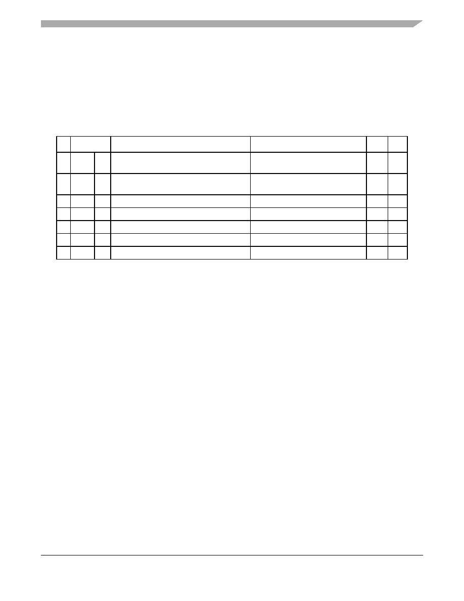
Table 9. Thermal Characteristics for 100-pin LQFP1
1 Thermal characteristics are targets based on simulation that are subject to change per device characterization.
No.
Symbol
Parameter
Conditions
Value Unit
1RθJA
CC Thermal resistance junction-to-ambient
natural convection2
2 Junction-to-Ambient thermal resistance determined per JEDEC JESD51-3 and JESD51-6. Thermal test board
meets JEDEC specification for this package.
Single layer board - 1s
TBD °C/W
2RθJMA CC Thermal resistance junction-to-ambient
natural convection2
Four layer board - 2s2p
TBD °C/W
3RθJA
CC Thermal resistance junction-to-ambient2
@ 200 ft./min., single layer board
TBD °C/W
@ 200 ft./min., four layer board 2s2p
TBD °C/W
5RθJB
CC Thermal resistance junction to board3
3 Junction-to-Board thermal resistance determined per JEDEC JESD51-8. Thermal test board meets JEDEC
specification for the specified package.
TBD °C/W
6RθJC
CC Thermal resistance junction to case4
4 Junction-to-Case at the top of the package determined using MIL-STD 883 Method 1012.1. The cold plate
temperature is used for the case temperature. Reported value includes the thermal resistance of the interface layer.
TBD °C/W
7
Ψ
JT
CC Junction to package top natural convection5
5 Thermal characterization parameter indicating the temperature difference between the package top and the junction
temperature per JEDEC JESD51-2. When Greek letters are not available, the thermal characterization parameter
is written as Psi-JT.
TBD °C/W
相關(guān)PDF資料 |
PDF描述 |
|---|---|
| MPC5602PEFMLL | MICROCONTROLLER, PQFP100 |
| MPC5603PEFMLQ | 32-BIT, FLASH, 64 MHz, MICROCONTROLLER, PQFP144 |
| MPC5603PEFMLL | 32-BIT, FLASH, 64 MHz, MICROCONTROLLER, PQFP100 |
| MPC603AFE66CB | 32-BIT, 66.67 MHz, RISC PROCESSOR, CQFP240 |
| MPC603AFE66CX | 32-BIT, 66.67 MHz, RISC PROCESSOR, CQFP240 |
相關(guān)代理商/技術(shù)參數(shù) |
參數(shù)描述 |
|---|---|
| MPC5602S | 制造商:FREESCALE 制造商全稱:Freescale Semiconductor, Inc 功能描述:MPC5606S Microcontroller Data Sheet |
| MPC5603B | 制造商:FREESCALE 制造商全稱:Freescale Semiconductor, Inc 功能描述:Qorivva MPC560xB/C/D Family |
| MPC5603BEMLL | 制造商:FREESCALE 制造商全稱:Freescale Semiconductor, Inc 功能描述:MPC5604B/C Microcontroller Data Sheet |
| MPC5603BEMLLR | 制造商:FREESCALE 制造商全稱:Freescale Semiconductor, Inc 功能描述:MPC5604B/C Microcontroller Data Sheet |
| MPC5603BEMLQ | 制造商:FREESCALE 制造商全稱:Freescale Semiconductor, Inc 功能描述:MPC5604B/C Microcontroller Data Sheet |
發(fā)布緊急采購(gòu),3分鐘左右您將得到回復(fù)。