- 您現(xiàn)在的位置:買賣IC網 > PDF目錄69036 > MPC5125YVN400 (FREESCALE SEMICONDUCTOR INC) 32-BIT, FLASH, 400 MHz, MICROCONTROLLER, PBGA324 PDF資料下載
參數(shù)資料
| 型號: | MPC5125YVN400 |
| 廠商: | FREESCALE SEMICONDUCTOR INC |
| 元件分類: | 微控制器/微處理器 |
| 英文描述: | 32-BIT, FLASH, 400 MHz, MICROCONTROLLER, PBGA324 |
| 封裝: | 23 X 23 MM, 2.25 MM HEIGHT, 1 MM PITCH, ROHS COMPLIANT, PLASTIC, MS-034AJJ-1, TEPBGA-324 |
| 文件頁數(shù): | 47/92頁 |
| 文件大小: | 640K |
| 代理商: | MPC5125YVN400 |
第1頁第2頁第3頁第4頁第5頁第6頁第7頁第8頁第9頁第10頁第11頁第12頁第13頁第14頁第15頁第16頁第17頁第18頁第19頁第20頁第21頁第22頁第23頁第24頁第25頁第26頁第27頁第28頁第29頁第30頁第31頁第32頁第33頁第34頁第35頁第36頁第37頁第38頁第39頁第40頁第41頁第42頁第43頁第44頁第45頁第46頁當前第47頁第48頁第49頁第50頁第51頁第52頁第53頁第54頁第55頁第56頁第57頁第58頁第59頁第60頁第61頁第62頁第63頁第64頁第65頁第66頁第67頁第68頁第69頁第70頁第71頁第72頁第73頁第74頁第75頁第76頁第77頁第78頁第79頁第80頁第81頁第82頁第83頁第84頁第85頁第86頁第87頁第88頁第89頁第90頁第91頁第92頁
Electrical and Thermal Characteristics
MPC5125 Microcontroller Data Sheet, Rev. 3
Freescale Semiconductor
51
4.3.5.1
DDR SDRAM AC Timing Specifications
4.3.5.2
MobileDDR/LPDDR SDRAM AC Timing Specifications
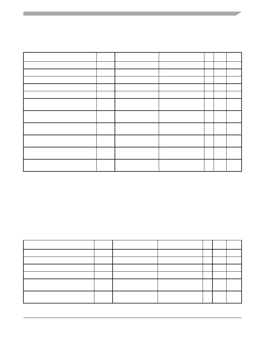
Table 21. DDR SDRAM Timing Specifications
At recommended operating conditions with VDD_IO_MEM of ±5%
Parameter
Symbol
Min
Max
Unit Notes SpecID
Clock cycle time, CL = x
tCK
6000
—
ps
A5.1
MCK AC differential crosspoint voltage
VOX-AC (VDD_IO_MEM × 0.5)– 0.15 (VDD_IO_MEM × 0.5) + 0.15
V
1
NOTES:
1 Measured with clock pin loaded with differential 100
Ω termination resistor.
A5.2
CK HIGH pulse width
tCH
0.47
0.53
tCK
A5.3
CK LOW pulse width
tCL
0.47
0.53
tCK
A5.4
Skew between MCK and DQS transitions
tDQSS
0.25
tCK
2,3
2 Measured with all outputs except the clock loaded with 50
Ω termination resistor to V
DD_IO_MEM/2.
3 All transitions measured at mid-supply (V
DD_IO_MEM/2).
A5.5
Address and control output setup time
relative to MCK rising edge
tOS(base)
tCK/2 – 1000
—
ps
A5.6
Address and control output hold time
relative to MCK rising edge
tOH(base)
tCK/2 – 1000
—
ps
A5.7
DQ and DM output setup time relative to
DQS
tDS1(base)
tCK/4 – 750
—
ps
A5.8
DQ and DM output hold time relative to
DQS
tDH1(base)
tCK/4 – 750
—
ps
A5.9
DQS-DQ skew for DQS and associated
DQ inputs
tDQSQ
– (tCK/4 – 600)
tCK/4 – 600
ps
A5.10
DQS window position related to CAS read
command
tDQSEN
2tCK + 1500
3tCK – 1000
ps 1,2,3,4,
5
4 In this window, the first rising edge of DQS should occur. From the start of the window to DQS rising edge, DQS should be low.
5 The window position is given for t
DQSEN = 2.0 tCK (RDLY = 2, HALF DQS DLY = QUART DQS DLY = 0) with CL = 3 DDR
SDRAM device. For other values of tDQSEN, the window position is shifted accordingly.
A5.11
Table 22. MobileDDR/LPDDR SDRAM Timing Specifications
At recommended operating conditions with VDD_IO_MEM of ±5%
Parameter
Symbol
Min
Max
Unit Notes SpecID
Clock cycle time, CL = x
tCK
6000
—
ps
A5.1
MCK AC differential crosspoint voltage
VOX-AC (VDD_IO_MEM × 0.5) – 0.1 (VDD_IO_MEM × 0.5) + 0.1
V
1
A5.2
CK HIGH pulse width
tCH
0.47
0.53
tCK
A5.3
CK LOW pulse width
tCL
0.47
0.53
tCK
A5.4
Skew between MCK and DQS
transitions
tDQSS
0.25
tCK
2,3
A5.5
Address and control output setup time
relative to MCK rising edge
tOS(base)
tCK/2 – 1000
—
ps
A5.6
相關PDF資料 |
PDF描述 |
|---|---|
| MPC5200CVR400B | 400 MHz, MICROPROCESSOR, PBGA272 |
| MPC5533MVZ80 | FLASH, 80 MHz, MICROCONTROLLER, PBGA324 |
| MPC5533MVM40 | FLASH, 40 MHz, MICROCONTROLLER, PBGA208 |
| MPC5533MZQ66 | FLASH, 66 MHz, MICROCONTROLLER, PBGA324 |
| MPC5533MVF80 | FLASH, 80 MHz, MICROCONTROLLER, PBGA208 |
相關代理商/技術參數(shù) |
參數(shù)描述 |
|---|---|
| MPC5125YVN400 | 制造商:Freescale Semiconductor 功能描述:ICMICROPROCESSOR32-BITCMOSPBGA324PI |
| MPC5125YVN400R | 制造商:Freescale Semiconductor 功能描述:POWERPC EMBEDDED SOC - Tape and Reel |
| MPC5200 | 制造商:FREESCALE 制造商全稱:Freescale Semiconductor, Inc 功能描述:Hardware Specifications |
| MPC5200B | 制造商:FREESCALE 制造商全稱:Freescale Semiconductor, Inc 功能描述:SDRAM/DDR Memory Controller |
| MPC5200B_08 | 制造商:FREESCALE 制造商全稱:Freescale Semiconductor, Inc 功能描述:SDRAM / DDR Memory Controller |
發(fā)布緊急采購,3分鐘左右您將得到回復。