- 您現(xiàn)在的位置:買賣IC網(wǎng) > PDF目錄359170 > ML4826IP-1 PFC and Dual Output PWM Controller Combo PDF資料下載
參數(shù)資料
| 型號: | ML4826IP-1 |
| 元件分類: | 基準電壓源/電流源 |
| 英文描述: | PFC and Dual Output PWM Controller Combo |
| 中文描述: | PFC和雙輸出PWM控制器組合 |
| 文件頁數(shù): | 11/16頁 |
| 文件大?。?/td> | 296K |
| 代理商: | ML4826IP-1 |

ML4826
11
Volts peak. The composite waveform feeding the RAMP2
pin for the PWM consists of the reflected output current
signal along with the transformer magnetizing current and
the slope compensation signal.
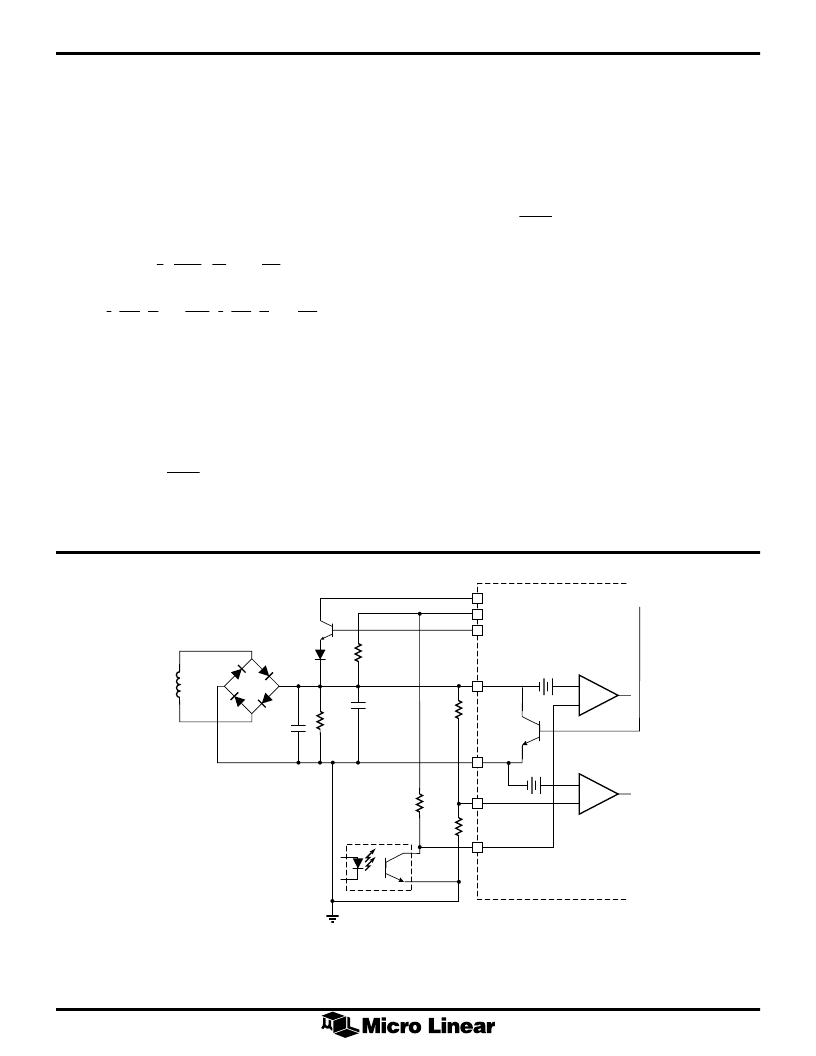
Equation 8 describes the composite signal feeding
RAMP2, consisting of the primary current of the main
transformer and the slope compensation. Equation 9
solves for the required slope compensation peak voltage.
V
I
V
L
N
N
T
n
V
V
RAMP
PRI
OUT
S
P
S
CT
FB
2
1
2
1
1 5
– .
=
+
×
×
×
×
≤
(8)
V
V
L
N
N
T
R
n
V
H
μ
V
SC
OUT
S
P
S
SENSE
CT
=
×
×
×
×
=
×
×
×
=
1
2
1
2
48
20
14
90
5
471
200
2 2
.
μ
sec
(9)
Soft Start
Start-up of the PWM is controlled by the selection of the
external capacitor at SS. A current source of 50
μ
A supplies
the charging current for the capacitor, and start-up of the
PWM begins at 1.5V. Start-up delay can be programmed
by the following equation:
C
t
A
V
SS
DELAY
=
×
50
1 5
.
μ
(10)
where C
SS
is the required soft start capacitance, and
t
DELAY
is the desired start-up delay.
It is important that the time constant of the PWM soft-start
allow the PFC time to generate sufficient output power for
the PWM section. The PWM start-up delay should be at
least 5ms.
Solving for the minimum value of C
SS
:
C
ms
5
A
V
nF
SS
=
×
=
50
1 5
.
167
μ
(11)
V
CC
The ML4826 is a current-fed part. It has an internal shunt
voltage regulator, which is designed to regulate the
voltage internal to the part at 13.5V. This allows a low
power dissipation while at the same time delivering 10V
of gate drive at the PWM OUT and PFC OUT outputs. It is
important to limit the current through the part to avoid
overheating or destroying the part.
There are a number of different ways to supply V
CC
to the
ML2826. The method suggested in Figure 5, is one which
keeps the ML4826 I
CC
current to a minimum, and allows
for a loosely regulated bootstrap winding. By feeding
external gate drive components from the base of Q1, the
constant current source does not have to account for
variations in the gate drive current. This helps to keep the
maximum I
CC
of the ML4826 to a minimum. Also, the
current available to charge the bootstrap capacitor from
the bootstrap winding is not limited by the constant
–
+
–
+
V
CC
V
REF
R
T
C
T
PWM CMP
DC I
LIMIT
1V
1.5V
R40
47.0k
R38
10.0k
R13
2.2k
RAMP2
AGND
DC I
LIMIT
V
DC
U2
R21
8.63k
Q14
2N2222
D1
R16
471
C11
1000pF
C26
220pF
T3
200:1
I
SENSE
x Former
4 x IN4148
6
10
11
9
7
18
17
Figure 4. Slope Compensation and Current Sense
FUNCTIONAL DESCRIPTION
(Continued)
相關(guān)PDF資料 |
PDF描述 |
|---|---|
| ML4826IP-2 | PFC and Dual Output PWM Controller Combo |
| ML4826CP2 | PFC and Dual Output PWM Controller Combo |
| ML4826 | PFC and Dual Output PWM Controller Combo |
| ML4827CP-1 | Fault-Protected PFC and PWM Controller Combo |
| ML4827CP-2 | Fault-Protected PFC and PWM Controller Combo |
相關(guān)代理商/技術(shù)參數(shù) |
參數(shù)描述 |
|---|---|
| ML4826IP2 | 制造商:Rochester Electronics LLC 功能描述:- Bulk |
| ML4826IP-2 | 制造商:MICRO-LINEAR 制造商全稱:MICRO-LINEAR 功能描述:PFC and Dual Output PWM Controller Combo |
| ML4826IS-1 | 制造商:MICRO-LINEAR 制造商全稱:MICRO-LINEAR 功能描述:PFC and Dual Output PWM Controller Combo |
| ML4826IS-2 | 制造商:MICRO-LINEAR 制造商全稱:MICRO-LINEAR 功能描述:PFC and Dual Output PWM Controller Combo |
| ML4827 | 制造商:MICRO-LINEAR 制造商全稱:MICRO-LINEAR 功能描述:Fault-Protected PFC and PWM Controller Combo |
發(fā)布緊急采購,3分鐘左右您將得到回復(fù)。