- 您現(xiàn)在的位置:買賣IC網(wǎng) > PDF目錄45328 > MK1492-04R (INTEGRATED DEVICE TECHNOLOGY INC) 75 MHz, PROC SPECIFIC CLOCK GENERATOR, PDSO28 PDF資料下載
參數(shù)資料
| 型號(hào): | MK1492-04R |
| 廠商: | INTEGRATED DEVICE TECHNOLOGY INC |
| 元件分類: | 時(shí)鐘產(chǎn)生/分配 |
| 英文描述: | 75 MHz, PROC SPECIFIC CLOCK GENERATOR, PDSO28 |
| 封裝: | 0.150 INCH, SSOP-28 |
| 文件頁數(shù): | 2/8頁 |
| 文件大小: | 102K |
| 代理商: | MK1492-04R |

MK1492-04
OPTi Firestar+ Clock Source
MDS1492-04C
2
Revision 4308
Printed 4/30/98
MicroClock Division of ICS1271 Parkmoor Ave.San JoseCA95126(408)295-9800tel(408)295-9818fax
PRELIMINARY INFORMATION
ICRO
CLOCK
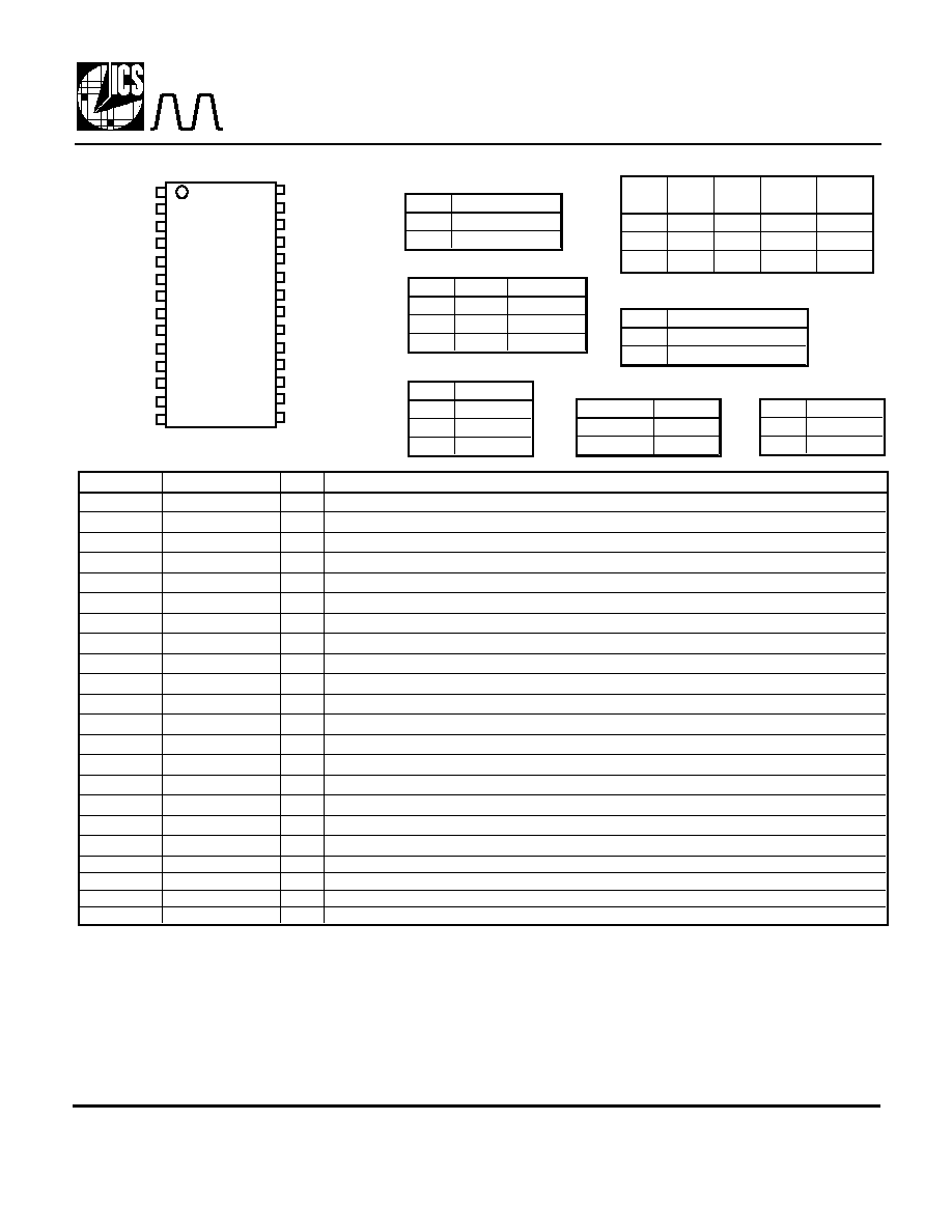
Pin #
Name
Type Description
1, 20, 26
VDD
P
Connect to +3.3V. Must be same voltage on all pins.
2
XI
I
Crystal connection. Connect to a 14.31818 MHz crystal or input clock.
3
XO
O
Crystal connection. Connect to a 14.31818 MHz crystal, or leave unconnected for clock.
4, 11, 17, 23
GND
P
Connect to Ground.
5
14.3(OE)
TI/O 14.318 MHz output. Amplitude matches VDD. Input control for tri-state of all clocks.
6
SDCLK
I
I C Serial Port Clock
7
SDATA
I
I C Serial Port Data
8
EHOST1
O
Early Host Output Clock 1. Amplitude matches VDD
. Auto adjusts to maintain drive.
9, 14
VDD
P
Connect to CPU VDD supply (3.3V or 2.5V).
10
HOST2
O
Host Output Clock 2. Amplitude matches VDD
. Auto adjusts to maintain strong drive.
12
HOST 3
O
Host Output Clock 3. No auto adjust.
13
HOST 4
O
Host Output Clock 4. No auto adjust.
15
CPUS#
TI
CPU Stop power down control; defined in table above. Signal connection on page 8.
16
PCISTP#
TI
PCI Stop power down control; defined in table above. Signal connection on page 8.
18
HOST 5,7
O
Host Output Clocks 5, 7. HOST7 enabled by DS input per table above.
19
HOST6,8(DS)
I/O
Host Output Clocks 6, 8 and DS input. HOST 8 enabled by DS input per table above.
21
48M/14.3M(SEL0)
I/O
Fixed frequency clock output and fixed frequency select input per table above.
22
PCIF(LE)
I/O
PCI Output clock that continues to run in PCI STOP mode. Low EMI enable input.
24
PCI(FS)
I/O
PCI Output clock, and CPU Frequency Select input. See PCIF and PCI tables above.
25
PCI(SEL1)
TI/O PCI Output clock, andSEL1 Select input. See PCIF and F1 tables above.
27
PCI(CSSS)
I/O
PCI output clock and CPU slow or stop mode select input per table above.
28
F1(PEN)
TI/O F1 clock output and PCIF Enable input.
Pin Descriptions
Host/PCI Frequency Select Table
Pin Assignment
1
8
9
2
3
4
5
6
7
10
11
12
13
14
16
15
20
17
18
19
25
24
23
22
21
26
27
28
VDDHOST1,2
SDATA
SDCLK
XO
VDD
14.3(OE)
HOST2
EHOST1
XI
GND
VDDHOST3,4
GND
HOST4
HOST3
HOST1,2 or 3,4
48M/14.3M Frequency
Select Table (MHz)
External Components
The MK1492 requires some inexpensive external components for proper operation. Decoupling capacitors of 0.1F should be connected on
each VDD pin to ground, as close to the MK1492 as possible. A series termination resistor of 33
may be used for each clock output. See the
discussion on page 8 for other external resistors required for proper I/O operation.
The 14.3 MHz oscillator has internal caps that provide the
proper load for a parallel resonant crystal with CL=12pF. For tuning with other values of CL, the formula 2*(CL-12) gives the value of each
capacitor that should be connected between X1 and ground and X2 and ground.
OE
ALL CLOCK OUTPUTS
0
TRISTATED
M, 1
ENABLED
Output Enable Control Table
SEL0
48M/14.3M
0
14.31818
1
48.0
EMI Control
LE
Low EMI
0
ON
1
OFF
HOST1,2
Key: I = Input, TI = tri-level input, O = Output, P = Power supply connection, (T)I/O = Input on power up, becomes an Output after 10ms.
Internal pull-up resistors are present on DS, SEL0, FS, LE, CPUS#, PCISTP#, and CSSS. Internal resistors on PEN, SEL1, and OE pull to a
mid-level (M).
SEL1
F1
0
PCI
M
14.318
1
24.0
F1 Frequency Select
VDD
PCIF(LE)
GND
VDD
F1(PEN)
HOST6,8(DS)
48M/14.3M(SEL0)
PCI(CSSS)
PCI(SEL1)
CPUS#
HOST5,7
PCISTP#
GND
PCI(FS)
PEN
Pin 25
Pin 24
0
PCI
M
PCI
PCIF
1
PCIF
PCIF Enable Control
OE=M
OE=1
CPUS#
CSSS
FS
HOST
1
X
0
60.0
50.0
1
X
1
66.66
75.0
M
0
X
33.33
DS
HOST7,8
0
ENABLED
1
TRISTATED
HOST7,8 Enable
2
HOST1,2
相關(guān)PDF資料 |
PDF描述 |
|---|---|
| MK1493-01G | 100 MHz, PROC SPECIFIC CLOCK GENERATOR, PDSO48 |
| MK1493-01G | 100 MHz, PROC SPECIFIC CLOCK GENERATOR, PDSO48 |
| MK1493-01GLF | 100 MHz, PROC SPECIFIC CLOCK GENERATOR, PDSO48 |
| MK1493-01GTR | 100 MHz, PROC SPECIFIC CLOCK GENERATOR, PDSO48 |
| MK1493-03BGILF | 100 MHz, PROC SPECIFIC CLOCK GENERATOR, PDSO48 |
相關(guān)代理商/技術(shù)參數(shù) |
參數(shù)描述 |
|---|---|
| MK1493-01 | 制造商:ICS 制造商全稱:ICS 功能描述:PCI Clock Generator |
| MK1493-01G | 制造商:ICS 制造商全稱:ICS 功能描述:PCI Clock Generator |
| MK1493-01GTR | 制造商:ICS 制造商全稱:ICS 功能描述:PCI Clock Generator |
| MK1493-03B | 制造商:IDT 制造商全稱:Integrated Device Technology 功能描述:PCI CLOCK GENERATOR |
| MK1493-03BGILF | 制造商:Integrated Device Technology Inc 功能描述:DIFFERENTIAL SPREAD SPECTRUM CLOCK DRIVER, TSSOP16 - Rail/Tube |
發(fā)布緊急采購,3分鐘左右您將得到回復(fù)。