- 您現(xiàn)在的位置:買賣IC網(wǎng) > PDF目錄67993 > MEGA32M1-ESMZ (ATMEL CORP) 8-BIT, FLASH, 16 MHz, RISC MICROCONTROLLER, QCC32 PDF資料下載
參數(shù)資料
| 型號: | MEGA32M1-ESMZ |
| 廠商: | ATMEL CORP |
| 元件分類: | 微控制器/微處理器 |
| 英文描述: | 8-BIT, FLASH, 16 MHz, RISC MICROCONTROLLER, QCC32 |
| 封裝: | 7 X 7 MM, 0.65 MM PITCH, LEAD FREE, MO-220VKKC, QFN-32 |
| 文件頁數(shù): | 244/365頁 |
| 文件大小: | 6391K |
| 代理商: | MEGA32M1-ESMZ |
第1頁第2頁第3頁第4頁第5頁第6頁第7頁第8頁第9頁第10頁第11頁第12頁第13頁第14頁第15頁第16頁第17頁第18頁第19頁第20頁第21頁第22頁第23頁第24頁第25頁第26頁第27頁第28頁第29頁第30頁第31頁第32頁第33頁第34頁第35頁第36頁第37頁第38頁第39頁第40頁第41頁第42頁第43頁第44頁第45頁第46頁第47頁第48頁第49頁第50頁第51頁第52頁第53頁第54頁第55頁第56頁第57頁第58頁第59頁第60頁第61頁第62頁第63頁第64頁第65頁第66頁第67頁第68頁第69頁第70頁第71頁第72頁第73頁第74頁第75頁第76頁第77頁第78頁第79頁第80頁第81頁第82頁第83頁第84頁第85頁第86頁第87頁第88頁第89頁第90頁第91頁第92頁第93頁第94頁第95頁第96頁第97頁第98頁第99頁第100頁第101頁第102頁第103頁第104頁第105頁第106頁第107頁第108頁第109頁第110頁第111頁第112頁第113頁第114頁第115頁第116頁第117頁第118頁第119頁第120頁第121頁第122頁第123頁第124頁第125頁第126頁第127頁第128頁第129頁第130頁第131頁第132頁第133頁第134頁第135頁第136頁第137頁第138頁第139頁第140頁第141頁第142頁第143頁第144頁第145頁第146頁第147頁第148頁第149頁第150頁第151頁第152頁第153頁第154頁第155頁第156頁第157頁第158頁第159頁第160頁第161頁第162頁第163頁第164頁第165頁第166頁第167頁第168頁第169頁第170頁第171頁第172頁第173頁第174頁第175頁第176頁第177頁第178頁第179頁第180頁第181頁第182頁第183頁第184頁第185頁第186頁第187頁第188頁第189頁第190頁第191頁第192頁第193頁第194頁第195頁第196頁第197頁第198頁第199頁第200頁第201頁第202頁第203頁第204頁第205頁第206頁第207頁第208頁第209頁第210頁第211頁第212頁第213頁第214頁第215頁第216頁第217頁第218頁第219頁第220頁第221頁第222頁第223頁第224頁第225頁第226頁第227頁第228頁第229頁第230頁第231頁第232頁第233頁第234頁第235頁第236頁第237頁第238頁第239頁第240頁第241頁第242頁第243頁當前第244頁第245頁第246頁第247頁第248頁第249頁第250頁第251頁第252頁第253頁第254頁第255頁第256頁第257頁第258頁第259頁第260頁第261頁第262頁第263頁第264頁第265頁第266頁第267頁第268頁第269頁第270頁第271頁第272頁第273頁第274頁第275頁第276頁第277頁第278頁第279頁第280頁第281頁第282頁第283頁第284頁第285頁第286頁第287頁第288頁第289頁第290頁第291頁第292頁第293頁第294頁第295頁第296頁第297頁第298頁第299頁第300頁第301頁第302頁第303頁第304頁第305頁第306頁第307頁第308頁第309頁第310頁第311頁第312頁第313頁第314頁第315頁第316頁第317頁第318頁第319頁第320頁第321頁第322頁第323頁第324頁第325頁第326頁第327頁第328頁第329頁第330頁第331頁第332頁第333頁第334頁第335頁第336頁第337頁第338頁第339頁第340頁第341頁第342頁第343頁第344頁第345頁第346頁第347頁第348頁第349頁第350頁第351頁第352頁第353頁第354頁第355頁第356頁第357頁第358頁第359頁第360頁第361頁第362頁第363頁第364頁第365頁
318
7647F–AVR–04/09
ATmega16/32/64/M1/C1
Note:
1. “Max” means the highest value where the pin is guaranteed to be read as low
2. “Min” means the lowest value where the pin is guaranteed to be read as high
3. Although each I/O port can sink more than the test conditions (10 mA at V
CC = 5V, 6 mA at VCC = 3V) under steady state
conditions (non-transient), the following must be observed:
1] The sum of all IOL, for ports B0 - B1, C2 - C3, D4, E1 - E2 should not exceed 70 mA.
2] The sum of all IOL, for ports B6 - B7, C0 - C1, D0 -D3, E0 should not exceed 70 mA.
3] The sum of all IOL, for ports B2 - B5, C4 - C7, D5 - D7 should not exceed 70 mA.
If IOL exceeds the test condition, VOL may exceed the related specification. Pins are not guaranteed to sink current greater
than the listed test condition.
4. Although each I/O port can source more than the test conditions (10 mA at
V
CC = 5V, 8 mA at VCC = 3V) under steady state
conditions (non-transient), the following must be observed:
1] The sum of all IOH, for ports B0 - B1, C2 - C3, D4, E1 - E2 should not exceed 100 mA.
2] The sum of all IOH, for ports B6 - B7, C0 - C1, D0 -D3, E0 should not exceed 100 mA.
3] The sum of all IOH, for ports B2 - B5, C4 - C7, D5 - D7 should not exceed 100 mA.
If IOH exceeds the test condition, VOH may exceed the related specification. Pins are not guaranteed to source current
greater than the listed test condition.
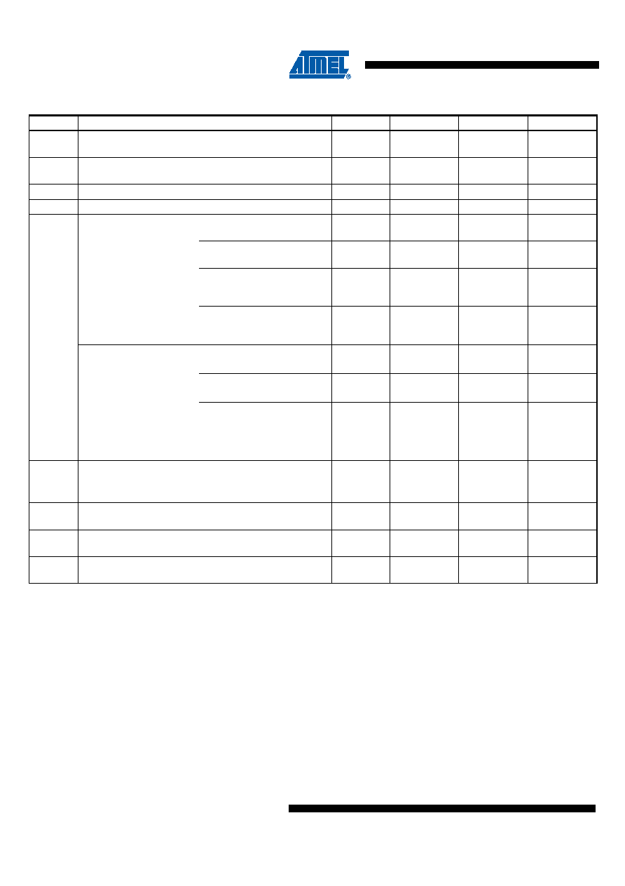
IIL
Input Leakage
Current I/O Pin
V
CC = 5.5V, pin low
(absolute value), except Port E
50
nA
IIH
Input Leakage
Current I/O Pin
V
CC = 5.5V, pin high
(absolute value), except Port E
50
nA
R
RST
Reset Pull-up Resistor
30
200
k
Ω
Rpu
I/O Pin Pull-up Resistor
20
50
k
Ω
ICC
Power Supply Current
Active 8 MHz, VCC = 3V, RC
osc, PRR = 0xFF
3.8
8
mA
Active 16 MHz, VCC = 5V, Ext
Clock, PRR = 0xFF
14
30
mA
Idle (16K and 32K devices)
VCC = 3V, F = 8 MHz
VCC = 5V, F = 16MHz
1.1
4.0
8
15
mA
Idle (64K devices only)
VCC = 3V, F = 8 MHz
VCC = 5V, F = 16MHz
1.5
5.8
8
15
mA
Power-down mode(5)
WDT enabled, VCC = 5V
t0 < 85°C
830
A
WDT enabled, VCC = 5V
85°C < t0 < 125°C
21
120
A
WDT disabled, VCC = 5V
t0 < 85°C
225
A
WDT disabled, VCC = 5V
85°C < t0 < 125°C
16
100
A
Vhysr
Analog Comparator
Hysteresis Voltage
VCC = 5V, Vin = 3V
Rising Edge
Falling Edge
-100
25
-35
70
mV
IACLK
Analog Comparator
Input Leakage Current
VCC = 5V
Vin = VCC/2
-50
+50
nA
tACID
Analog Comparator
Propagation Delay
VCC = 2.7V
VCC = 5.0V
(6)
ns
ISRC
Current Source Value
VCC = 5V: Max Rload 30 KΩ
VCC = 3V: Max Rload 15 KΩ
95
100
105
A
T
A = -40° C to +125° C, VCC = 2.7V to 5.5V (unless otherwise noted) (Continued)
Symbol
Parameter
Condition
Min.
Typ.
Max.
Units
相關PDF資料 |
PDF描述 |
|---|---|
| MEGA64C1-ESMZ | 8-BIT, FLASH, 16 MHz, RISC MICROCONTROLLER, QCC32 |
| MIC74YQSTR | 8 I/O, PIA-GENERAL PURPOSE, PDSO16 |
| MIC74YQS | 8 I/O, PIA-GENERAL PURPOSE, PDSO16 |
| MJ80C51XXX/B:D | 8-BIT, MROM, 12 MHz, MICROCONTROLLER, PQCC44 |
| IT80C31-L | 8-BIT, 6 MHz, MICROCONTROLLER, PQFP44 |
相關代理商/技術參數(shù) |
參數(shù)描述 |
|---|---|
| MEGA48A-MMH SL383 | 制造商:Atmel Corporation 功能描述:IC MCU 8BIT 4KB FLASH 28VQFN |
| MEGA48PA-CCU SL383 | 制造商:Atmel Corporation 功能描述:IC MCU 8BIT 4KB FLASH 32UFBGA |
| MEGA64C1-15AZ | 制造商:ATMEL 制造商全稱:ATMEL Corporation 功能描述:8-bit Microcontroller with 16K/32K/64K Bytes In-System Programmable Flash |
| MEGA64C1-15MZ | 制造商:ATMEL 制造商全稱:ATMEL Corporation 功能描述:8-bit Microcontroller with 16K/32K/64K Bytes In-System Programmable Flash |
| MEGA64C1-ESAZ | 制造商:ATMEL 制造商全稱:ATMEL Corporation 功能描述:8-bit Microcontroller with 16K/32K/64K Bytes In-System Programmable Flash |
發(fā)布緊急采購,3分鐘左右您將得到回復。