- 您現(xiàn)在的位置:買賣IC網(wǎng) > PDF目錄296503 > MCP631-E/SN OP-AMP, 8000 uV OFFSET-MAX, 24 MHz BAND WIDTH, PDSO8 PDF資料下載
參數(shù)資料
| 型號: | MCP631-E/SN |
| 元件分類: | 運算放大器 |
| 英文描述: | OP-AMP, 8000 uV OFFSET-MAX, 24 MHz BAND WIDTH, PDSO8 |
| 封裝: | 3.90 MM, ROHS COMPLIANT, PLASTIC, SOIC-8 |
| 文件頁數(shù): | 14/42頁 |
| 文件大小: | 790K |
| 代理商: | MCP631-E/SN |
第1頁第2頁第3頁第4頁第5頁第6頁第7頁第8頁第9頁第10頁第11頁第12頁第13頁當前第14頁第15頁第16頁第17頁第18頁第19頁第20頁第21頁第22頁第23頁第24頁第25頁第26頁第27頁第28頁第29頁第30頁第31頁第32頁第33頁第34頁第35頁第36頁第37頁第38頁第39頁第40頁第41頁第42頁
2009 Microchip Technology Inc.
DS22197A-page 21
MCP631/2/3/5
4.0
APPLICATIONS
The MCP631/2/3/5 family op amps is manufactured
using Microchip’s state of the art CMOS process. It is
designed for low cost, low power and high speed
applications. Its low supply voltage, low quiescent
current and wide bandwidth make the MCP631/2/3/5
ideal for battery-powered applications.
4.1
Input
4.1.1
PHASE REVERSAL
The input devices are designed to not exhibit phase
inversion when the input pins exceed the supply
voltages.
shows
an
input
voltage
exceeding both supplies with no phase inversion.
4.1.2
INPUT VOLTAGE AND CURRENT
LIMITS
The ESD protection on the inputs can be depicted as
shown in Figure 4-1. This structure was chosen to
protect the input transistors, and to minimize input bias
current (IB). The input ESD diodes clamp the inputs
when they try to go more than one diode drop below
VSS. They also clamp any voltages that go too far
above VDD; their breakdown voltage is high enough to
allow normal operation, and low enough to bypass
quick ESD events within the specified limits.
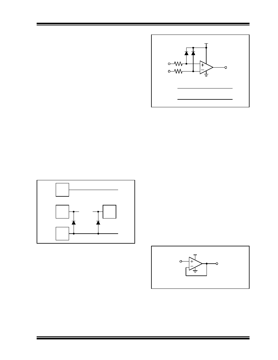
FIGURE 4-1:
Simplified Analog Input ESD
Structures.
In order to prevent damage and/or improper operation
of these amplifiers, the circuit must limit the currents
(and voltages) at the input pins (see Section 1.1
the recommended approach to protecting these inputs.
The internal ESD diodes prevent the input pins
(VIN+ and VIN–) from going too far below ground, and
the resistors R1 and R2 limit the possible current drawn
out of the input pins. Diodes D1 and D2 prevent the
input pins (VIN+ and VIN–) from going too far above
VDD, and dump any currents onto VDD. When
implemented as shown, resistors R1 and R2 also limit
the current through D1 and D2.
FIGURE 4-2:
Protecting the Analog
Inputs.
It is also possible to connect the diodes to the left of the
resistor R1 and R2. In this case, the currents through
the diodes D1 and D2 need to be limited by some other
mechanism. The resistors then serve as in-rush
current limiters; the DC current into the input pins
(VIN+ and VIN–) should be very small.
A significant amount of current can flow out of the
inputs (through the ESD diodes) when the common
mode voltage (VCM) is below ground (VSS); see
Figure 2-13. Applications that are high impedance may
need to limit the usable voltage range.
4.1.3
NORMAL OPERATION
The input stage of the MCP631/2/3/5 op amps uses a
differential PMOS input stage. It operates at
low common mode input voltages (VCM), with VCM
between VSS – 0.3V and VDD – 1.3V. To ensure proper
operation, the input offset voltage (VOS) is measured
at both
VCM =VSS – 0.3V
and
VDD –1.3V.
See Figure 2-5 and Figure 2-6 for temperature effects.
When operating at very low non-inverting gains, the
output voltage is limited at the top by the VCM range
FIGURE 4-3:
Unity Gain Voltage
Limitations for Linear Operation.
Bond
Pad
Bond
Pad
Bond
Pad
VDD
VIN+
VSS
Input
Stage
Bond
Pad
VIN–
V1
R1
VDD
D1
R1 >
VSS – (minimum expected V1)
2mA
VOUT
R2 >
VSS – (minimum expected V2)
2mA
V2
R2
D2
MCP63X
VIN
VDD
VOUT
V
SS
V
<
IN
V
,
OUT
V
DD
1.3V
–
≤
MCP63X
相關PDF資料 |
PDF描述 |
|---|---|
| MCP631T-E/SN | OP-AMP, 8000 uV OFFSET-MAX, 24 MHz BAND WIDTH, PDSO8 |
| MCP73832-4ADI/OT | 1-CHANNEL POWER SUPPLY SUPPORT CKT, PDSO5 |
| MCP73832-5DCI/MC | 1-CHANNEL POWER SUPPLY SUPPORT CKT, PDSO8 |
| MCR264-4-AC | 40 A, 200 V, SCR, TO-220AB |
| MCR68-6-BC | 12 A, 400 V, SCR, TO-220AB |
相關代理商/技術參數(shù) |
參數(shù)描述 |
|---|---|
| MCP631T-E/MNY | 功能描述:運算放大器 - 運放 Single 24MHz OP E temp RoHS:否 制造商:STMicroelectronics 通道數(shù)量:4 共模抑制比(最小值):63 dB 輸入補償電壓:1 mV 輸入偏流(最大值):10 pA 工作電源電壓:2.7 V to 5.5 V 安裝風格:SMD/SMT 封裝 / 箱體:QFN-16 轉換速度:0.89 V/us 關閉:No 輸出電流:55 mA 最大工作溫度:+ 125 C 封裝:Reel |
| MCP631T-E/OT | 功能描述:運算放大器 - 運放 Single 24MHz OP E temp RoHS:否 制造商:STMicroelectronics 通道數(shù)量:4 共模抑制比(最小值):63 dB 輸入補償電壓:1 mV 輸入偏流(最大值):10 pA 工作電源電壓:2.7 V to 5.5 V 安裝風格:SMD/SMT 封裝 / 箱體:QFN-16 轉換速度:0.89 V/us 關閉:No 輸出電流:55 mA 最大工作溫度:+ 125 C 封裝:Reel |
| MCP631T-E/SN | 功能描述:運算放大器 - 運放 Single 24MHz OP E temp RoHS:否 制造商:STMicroelectronics 通道數(shù)量:4 共模抑制比(最小值):63 dB 輸入補償電壓:1 mV 輸入偏流(最大值):10 pA 工作電源電壓:2.7 V to 5.5 V 安裝風格:SMD/SMT 封裝 / 箱體:QFN-16 轉換速度:0.89 V/us 關閉:No 輸出電流:55 mA 最大工作溫度:+ 125 C 封裝:Reel |
| MCP632-E/MF | 功能描述:運算放大器 - 運放 Dual 24MHz OP E temp RoHS:否 制造商:STMicroelectronics 通道數(shù)量:4 共模抑制比(最小值):63 dB 輸入補償電壓:1 mV 輸入偏流(最大值):10 pA 工作電源電壓:2.7 V to 5.5 V 安裝風格:SMD/SMT 封裝 / 箱體:QFN-16 轉換速度:0.89 V/us 關閉:No 輸出電流:55 mA 最大工作溫度:+ 125 C 封裝:Reel |
| MCP632-E/SN | 功能描述:運算放大器 - 運放 Dual 24MHz OP E temp RoHS:否 制造商:STMicroelectronics 通道數(shù)量:4 共模抑制比(最小值):63 dB 輸入補償電壓:1 mV 輸入偏流(最大值):10 pA 工作電源電壓:2.7 V to 5.5 V 安裝風格:SMD/SMT 封裝 / 箱體:QFN-16 轉換速度:0.89 V/us 關閉:No 輸出電流:55 mA 最大工作溫度:+ 125 C 封裝:Reel |
發(fā)布緊急采購,3分鐘左右您將得到回復。