- 您現(xiàn)在的位置:買賣IC網(wǎng) > PDF目錄378669 > MCM67H618BFN9 (MOTOROLA INC) 64K x 18 Bit BurstRAM Synchronous Fast Static RAM PDF資料下載
參數(shù)資料
| 型號: | MCM67H618BFN9 |
| 廠商: | MOTOROLA INC |
| 元件分類: | DRAM |
| 英文描述: | 64K x 18 Bit BurstRAM Synchronous Fast Static RAM |
| 中文描述: | 64K X 18 CACHE SRAM, 9 ns, PQCC52 |
| 封裝: | PLASTIC, LCC-52 |
| 文件頁數(shù): | 5/12頁 |
| 文件大小: | 167K |
| 代理商: | MCM67H618BFN9 |
MCM67H618B
5
MOTOROLA FAST SRAM
AC OPERATING CONDITIONS AND CHARACTERISTICS
(VCC = 5.0 V
±
5%, TA = 0 to + 70
°
C, Unless Otherwise Noted)
Input Timing Measurement Reference Level
Input Pulse Levels
. . . . . . . . . . . . . . . . . . . . . . . . . . . . . . . . .
Input Rise/Fall Time
. . . . . . . . . . . . . . . . . . . . . . . . . . . . . . . . . . . .
1.5 V
. . . . . . . . . . . . . . .
0 to 3.0 V
3 ns
Output Timing Reference Level
Output Load
. . . . . . . . . . . . . .
1.5 V
. . . . . . . . . . . . . . . . . . . . . . . . . .
See Figure 1 Unless Otherwise Noted
READ/WRITE CYCLE TIMING
(See Notes 1, 2, 3, and 4)
Parameter
Symbol
b l
MCM67H618B–9
MCM67H618B–10
MCM67H618B–12
U i
Unit
Notes
Min
Max
Min
Max
Min
Max
Cycle Time
tKHKH
tKHQV
tGLQV
tKHQX1
tKHQX2
tGLQX
tGHQZ
tKHQZ
tKHKL
tKLKH
tAVKH
tADSVKH
tDVKH
tWVKH
tADVVKH
tEVKH
15
—
16.6
—
20
—
ns
Clock Access Time
—
9
—
10
—
12
ns
5
Output Enable to Output Valid
—
5
—
5
—
6
ns
Clock High to Output Active
6
—
6
—
6
—
ns
Clock High to Output Change
3
—
3
—
3
—
ns
Output Enable to Output Active
0
—
0
—
0
—
ns
Output Disable to Q High–Z
—
6
—
7
—
7
ns
6
Clock High to Q High–Z
3
6
3
7
3
7
ns
Clock High Pulse Width
5
—
5
—
6
—
ns
Clock Low Pulse Width
5
—
5
—
6
—
ns
Setup Times:
Address
Address Status
Data In
Write
Address Advance
Chip Enable
2.5
—
2.5
—
2.5
—
ns
7
Hold Times:
Address
Address Status
Data In
Write
Address Advance
Chip Enable
tKHAX
tKHADSX
tKHDX
tKHWX
tKHADVX
tKHEX
0.5
—
0.5
—
0.5
—
ns
7
NOTES:
1. In setup and hold times, W (write) refers to either one or both byte write enables LW and UW.
2. A read cycle is defined by UW and LW high or ADSP low for the setup and hold times. A write cycle is defined by LW or UW low and ADSP
high for the setup and hold times.
3. All read and write cycle timings are referenced from K or G.
4. G is a don’t care when UW or LW is sampled low.
5. Maximum access times are guaranteed for all possible i486 and Pentium external bus cycles.
6. Transition is measured
±
500 mV from steady–state voltage. This parameter is sampled rather than 100% tested. At any given voltage and
temperature, tKHQZ max is less than tKHQZ1 min for a given device and from device to device.
7. This is a synchronous device. All addresses must meet the specified setup and hold times for
ALL
rising edges of K whenever ADSP
or ADSC is low, and the chip is selected. All other synchronous inputs must meet the specified setup and hold times for
ALL
rising
edges of K when the chip is enabled. Chip enable must be asserted at each rising edge of clock for the device (when ADSC is low) to remain
enabled.
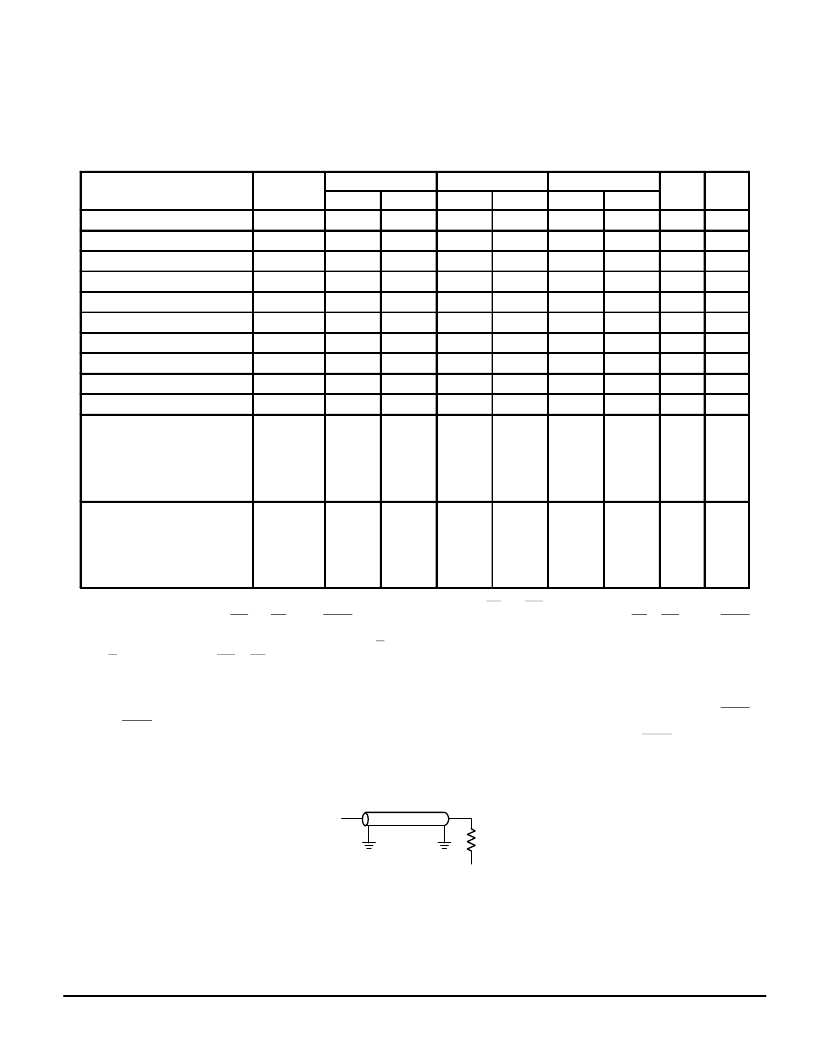
Figure 1. Test Load
OUTPUT
Z0 = 50
RL = 50
VL = 1.5 V
相關(guān)PDF資料 |
PDF描述 |
|---|---|
| MCM67Q709AZP10 | 128K x 9 Bit Separate I/O Synchronous Fast Static RAM |
| MCM67Q709AZP10R | 128K x 9 Bit Separate I/O Synchronous Fast Static RAM |
| MCM72F7ADG10 | 512KB and 1MB Synchronous Fast Static RAM Module |
| MCM72F7ADG12 | 512KB and 1MB Synchronous Fast Static RAM Module |
| MCM72F7ADG9 | 512KB and 1MB Synchronous Fast Static RAM Module |
相關(guān)代理商/技術(shù)參數(shù) |
參數(shù)描述 |
|---|---|
| MCM67J518 | 制造商:MOTOROLA 制造商全稱:Motorola, Inc 功能描述:32K x 18 Bit BurstRAM Synchronous Fast Static RA |
| MCM67J518FN6 | 制造商:MOTOROLA 制造商全稱:Motorola, Inc 功能描述:32K x 18 Bit BurstRAM Synchronous Fast Static RA |
| MCM67J518FN7 | 制造商:MOTOROLA 制造商全稱:Motorola, Inc 功能描述:32K x 18 Bit BurstRAM Synchronous Fast Static RA |
| MCM67J518FN9 | 制造商:MOTOROLA 制造商全稱:Motorola, Inc 功能描述:32K x 18 Bit BurstRAM Synchronous Fast Static RA |
| MCM67J618B | 制造商:MOTOROLA 制造商全稱:Motorola, Inc 功能描述:64K x 18 Bit BurstRAM Synchronous Fast Static RAM |
發(fā)布緊急采購,3分鐘左右您將得到回復(fù)。