- 您現(xiàn)在的位置:買賣IC網(wǎng) > PDF目錄359141 > MC68HC08GT16 (飛思卡爾半導(dǎo)體(中國(guó))有限公司) 8-bit microcontroller(8位MCU) PDF資料下載
參數(shù)資料
| 型號(hào): | MC68HC08GT16 |
| 廠商: | 飛思卡爾半導(dǎo)體(中國(guó))有限公司 |
| 英文描述: | 8-bit microcontroller(8位MCU) |
| 中文描述: | 8位微控制器(8位微控制器) |
| 文件頁(yè)數(shù): | 247/292頁(yè) |
| 文件大小: | 3759K |
| 代理商: | MC68HC08GT16 |
第1頁(yè)第2頁(yè)第3頁(yè)第4頁(yè)第5頁(yè)第6頁(yè)第7頁(yè)第8頁(yè)第9頁(yè)第10頁(yè)第11頁(yè)第12頁(yè)第13頁(yè)第14頁(yè)第15頁(yè)第16頁(yè)第17頁(yè)第18頁(yè)第19頁(yè)第20頁(yè)第21頁(yè)第22頁(yè)第23頁(yè)第24頁(yè)第25頁(yè)第26頁(yè)第27頁(yè)第28頁(yè)第29頁(yè)第30頁(yè)第31頁(yè)第32頁(yè)第33頁(yè)第34頁(yè)第35頁(yè)第36頁(yè)第37頁(yè)第38頁(yè)第39頁(yè)第40頁(yè)第41頁(yè)第42頁(yè)第43頁(yè)第44頁(yè)第45頁(yè)第46頁(yè)第47頁(yè)第48頁(yè)第49頁(yè)第50頁(yè)第51頁(yè)第52頁(yè)第53頁(yè)第54頁(yè)第55頁(yè)第56頁(yè)第57頁(yè)第58頁(yè)第59頁(yè)第60頁(yè)第61頁(yè)第62頁(yè)第63頁(yè)第64頁(yè)第65頁(yè)第66頁(yè)第67頁(yè)第68頁(yè)第69頁(yè)第70頁(yè)第71頁(yè)第72頁(yè)第73頁(yè)第74頁(yè)第75頁(yè)第76頁(yè)第77頁(yè)第78頁(yè)第79頁(yè)第80頁(yè)第81頁(yè)第82頁(yè)第83頁(yè)第84頁(yè)第85頁(yè)第86頁(yè)第87頁(yè)第88頁(yè)第89頁(yè)第90頁(yè)第91頁(yè)第92頁(yè)第93頁(yè)第94頁(yè)第95頁(yè)第96頁(yè)第97頁(yè)第98頁(yè)第99頁(yè)第100頁(yè)第101頁(yè)第102頁(yè)第103頁(yè)第104頁(yè)第105頁(yè)第106頁(yè)第107頁(yè)第108頁(yè)第109頁(yè)第110頁(yè)第111頁(yè)第112頁(yè)第113頁(yè)第114頁(yè)第115頁(yè)第116頁(yè)第117頁(yè)第118頁(yè)第119頁(yè)第120頁(yè)第121頁(yè)第122頁(yè)第123頁(yè)第124頁(yè)第125頁(yè)第126頁(yè)第127頁(yè)第128頁(yè)第129頁(yè)第130頁(yè)第131頁(yè)第132頁(yè)第133頁(yè)第134頁(yè)第135頁(yè)第136頁(yè)第137頁(yè)第138頁(yè)第139頁(yè)第140頁(yè)第141頁(yè)第142頁(yè)第143頁(yè)第144頁(yè)第145頁(yè)第146頁(yè)第147頁(yè)第148頁(yè)第149頁(yè)第150頁(yè)第151頁(yè)第152頁(yè)第153頁(yè)第154頁(yè)第155頁(yè)第156頁(yè)第157頁(yè)第158頁(yè)第159頁(yè)第160頁(yè)第161頁(yè)第162頁(yè)第163頁(yè)第164頁(yè)第165頁(yè)第166頁(yè)第167頁(yè)第168頁(yè)第169頁(yè)第170頁(yè)第171頁(yè)第172頁(yè)第173頁(yè)第174頁(yè)第175頁(yè)第176頁(yè)第177頁(yè)第178頁(yè)第179頁(yè)第180頁(yè)第181頁(yè)第182頁(yè)第183頁(yè)第184頁(yè)第185頁(yè)第186頁(yè)第187頁(yè)第188頁(yè)第189頁(yè)第190頁(yè)第191頁(yè)第192頁(yè)第193頁(yè)第194頁(yè)第195頁(yè)第196頁(yè)第197頁(yè)第198頁(yè)第199頁(yè)第200頁(yè)第201頁(yè)第202頁(yè)第203頁(yè)第204頁(yè)第205頁(yè)第206頁(yè)第207頁(yè)第208頁(yè)第209頁(yè)第210頁(yè)第211頁(yè)第212頁(yè)第213頁(yè)第214頁(yè)第215頁(yè)第216頁(yè)第217頁(yè)第218頁(yè)第219頁(yè)第220頁(yè)第221頁(yè)第222頁(yè)第223頁(yè)第224頁(yè)第225頁(yè)第226頁(yè)第227頁(yè)第228頁(yè)第229頁(yè)第230頁(yè)第231頁(yè)第232頁(yè)第233頁(yè)第234頁(yè)第235頁(yè)第236頁(yè)第237頁(yè)第238頁(yè)第239頁(yè)第240頁(yè)第241頁(yè)第242頁(yè)第243頁(yè)第244頁(yè)第245頁(yè)第246頁(yè)當(dāng)前第247頁(yè)第248頁(yè)第249頁(yè)第250頁(yè)第251頁(yè)第252頁(yè)第253頁(yè)第254頁(yè)第255頁(yè)第256頁(yè)第257頁(yè)第258頁(yè)第259頁(yè)第260頁(yè)第261頁(yè)第262頁(yè)第263頁(yè)第264頁(yè)第265頁(yè)第266頁(yè)第267頁(yè)第268頁(yè)第269頁(yè)第270頁(yè)第271頁(yè)第272頁(yè)第273頁(yè)第274頁(yè)第275頁(yè)第276頁(yè)第277頁(yè)第278頁(yè)第279頁(yè)第280頁(yè)第281頁(yè)第282頁(yè)第283頁(yè)第284頁(yè)第285頁(yè)第286頁(yè)第287頁(yè)第288頁(yè)第289頁(yè)第290頁(yè)第291頁(yè)第292頁(yè)
Monitor Module (MON)
MC68HC908GT16 MC68HC908GT8 MC68HC08GT16 Data Sheet, Rev. 5.0
Freescale Semiconductor
247
19.3.1.1 Normal Monitor Mode
When V
TST
is applied to IRQ and PTC3 is low upon monitor mode entry, the bus frequency is a
divide-by-two of the input clock. If PTC3 is high with V
TST
applied to IRQ upon monitor mode entry, the
bus frequency will be a divide-by-four of the input clock. Holding the PTC3 pin low when entering monitor
mode causes a bypass of a divide-by-two stage at the oscillator
only if V
TST
is applied to IRQ
. In this
event, the CGMOUT frequency is equal to the CGMXCLK frequency, and the OSC1 input directly
generates internal bus clocks. In this case, the OSC1 signal must have a 50% duty cycle at maximum bus
frequency.
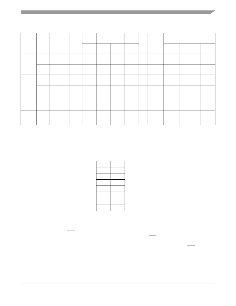
Table 19-1. Monitor Mode Signal Requirements and Options
Mode
IRQ
RST
Reset
Vector
Serial
Comm.
Mode Selection Divider
ICG
COP
Communication Speed
PTA0
PTC0
PTC1
PTC3
External
Clock
Bus
Frequency
Baud
Range
Normal
Monitor
V
TST
V
DD
or V
SS
X
1
1
0
0
OFF Disabled
4.9152
MHz
2.4576
MHz
9600
V
TST
V
DD
or V
SS
X
1
1
0
1
OFF Disabled
9.8304
MHz
2.4576
MHz
9600
Forced
Monitor
V
DD
V
DD
$FFFF
(blank)
1
X
X
X
OFF Disabled
9.8304
MHz
2.4576
MHz
9600
V
SS
V
DD
$FFFF
(blank)
1
X
X
X
ON Disabled
X
Nominal
2.4576
MHz
Nominal
9600
User
V
DD
or V
SS
V
DD
or V
SS
Not
$FFFF
X
X
X
X
X
Enabled
X
X
X
MON08
Function
[Pin No.]
V
TST
[6]
RST
[4]
—
COM
[8]
MOD0
[12]
MOD1
[14]
DIV4
[16]
—
—
OSC1
[13]
—
—
1. PTA0 must have a pullup resistor to VDD in monitor mode.
2. Communication speed in the table is an example to obtain a baud rate of 9600.
Baud rate using external oscillator is bus frequency / 256.
3. External clock is a 4.1952 MHz or 9.8304 MHz canned oscillator on OSC1.
4. X = don’t care.
5. MON08 pin refers to P&E Microcomputer Systems’ MONOUT-Cyclone 2 by 8-pin connector.
NC
1
2
GND
NC
3
4
RST
NC
5
6
IRQ
NC
7
8
PTA0
NC
9
10
NC
NC
11
12
PTC0
OSC1
13
14
PTC1
V
DD
15
16
PTC3
相關(guān)PDF資料 |
PDF描述 |
|---|---|
| MC68HC08JK3EMDW | Microcontrollers |
| MC68HC08JK8CDW | Microcontrollers |
| MC68HC08JL3H | Microcontrollers |
| MC68HC08JT8 | M68HC08 Microcontrollers |
| MC68HC08KH12A | Microcontrollers |
相關(guān)代理商/技術(shù)參數(shù) |
參數(shù)描述 |
|---|---|
| MC68HC08GZ32 | 制造商:FREESCALE 制造商全稱:Freescale Semiconductor, Inc 功能描述:Microcontrollers |
| MC68HC08GZ32CFA | 制造商:FREESCALE 制造商全稱:Freescale Semiconductor, Inc 功能描述:Microcontrollers |
| MC68HC08GZ32CFJ | 制造商:FREESCALE 制造商全稱:Freescale Semiconductor, Inc 功能描述:Microcontrollers |
| MC68HC08GZ32CFU | 制造商:FREESCALE 制造商全稱:Freescale Semiconductor, Inc 功能描述:Microcontrollers |
| MC68HC08GZ32MFA | 制造商:FREESCALE 制造商全稱:Freescale Semiconductor, Inc 功能描述:Microcontrollers |
發(fā)布緊急采購(gòu),3分鐘左右您將得到回復(fù)。