- 您現(xiàn)在的位置:買賣IC網(wǎng) > PDF目錄98012 > MC68HC08AS32FN (FREESCALE SEMICONDUCTOR INC) 8-BIT, EEPROM, 8.4 MHz, MICROCONTROLLER, PQCC52 PDF資料下載
參數(shù)資料
| 型號(hào): | MC68HC08AS32FN |
| 廠商: | FREESCALE SEMICONDUCTOR INC |
| 元件分類: | 微控制器/微處理器 |
| 英文描述: | 8-BIT, EEPROM, 8.4 MHz, MICROCONTROLLER, PQCC52 |
| 封裝: | PLASTIC, LCC-52 |
| 文件頁數(shù): | 67/280頁 |
| 文件大?。?/td> | 3453K |
| 代理商: | MC68HC08AS32FN |
第1頁第2頁第3頁第4頁第5頁第6頁第7頁第8頁第9頁第10頁第11頁第12頁第13頁第14頁第15頁第16頁第17頁第18頁第19頁第20頁第21頁第22頁第23頁第24頁第25頁第26頁第27頁第28頁第29頁第30頁第31頁第32頁第33頁第34頁第35頁第36頁第37頁第38頁第39頁第40頁第41頁第42頁第43頁第44頁第45頁第46頁第47頁第48頁第49頁第50頁第51頁第52頁第53頁第54頁第55頁第56頁第57頁第58頁第59頁第60頁第61頁第62頁第63頁第64頁第65頁第66頁當(dāng)前第67頁第68頁第69頁第70頁第71頁第72頁第73頁第74頁第75頁第76頁第77頁第78頁第79頁第80頁第81頁第82頁第83頁第84頁第85頁第86頁第87頁第88頁第89頁第90頁第91頁第92頁第93頁第94頁第95頁第96頁第97頁第98頁第99頁第100頁第101頁第102頁第103頁第104頁第105頁第106頁第107頁第108頁第109頁第110頁第111頁第112頁第113頁第114頁第115頁第116頁第117頁第118頁第119頁第120頁第121頁第122頁第123頁第124頁第125頁第126頁第127頁第128頁第129頁第130頁第131頁第132頁第133頁第134頁第135頁第136頁第137頁第138頁第139頁第140頁第141頁第142頁第143頁第144頁第145頁第146頁第147頁第148頁第149頁第150頁第151頁第152頁第153頁第154頁第155頁第156頁第157頁第158頁第159頁第160頁第161頁第162頁第163頁第164頁第165頁第166頁第167頁第168頁第169頁第170頁第171頁第172頁第173頁第174頁第175頁第176頁第177頁第178頁第179頁第180頁第181頁第182頁第183頁第184頁第185頁第186頁第187頁第188頁第189頁第190頁第191頁第192頁第193頁第194頁第195頁第196頁第197頁第198頁第199頁第200頁第201頁第202頁第203頁第204頁第205頁第206頁第207頁第208頁第209頁第210頁第211頁第212頁第213頁第214頁第215頁第216頁第217頁第218頁第219頁第220頁第221頁第222頁第223頁第224頁第225頁第226頁第227頁第228頁第229頁第230頁第231頁第232頁第233頁第234頁第235頁第236頁第237頁第238頁第239頁第240頁第241頁第242頁第243頁第244頁第245頁第246頁第247頁第248頁第249頁第250頁第251頁第252頁第253頁第254頁第255頁第256頁第257頁第258頁第259頁第260頁第261頁第262頁第263頁第264頁第265頁第266頁第267頁第268頁第269頁第270頁第271頁第272頁第273頁第274頁第275頁第276頁第277頁第278頁第279頁第280頁
MC68HC08AS32 — Rev. 4.1
Data Sheet
Freescale Semiconductor
159
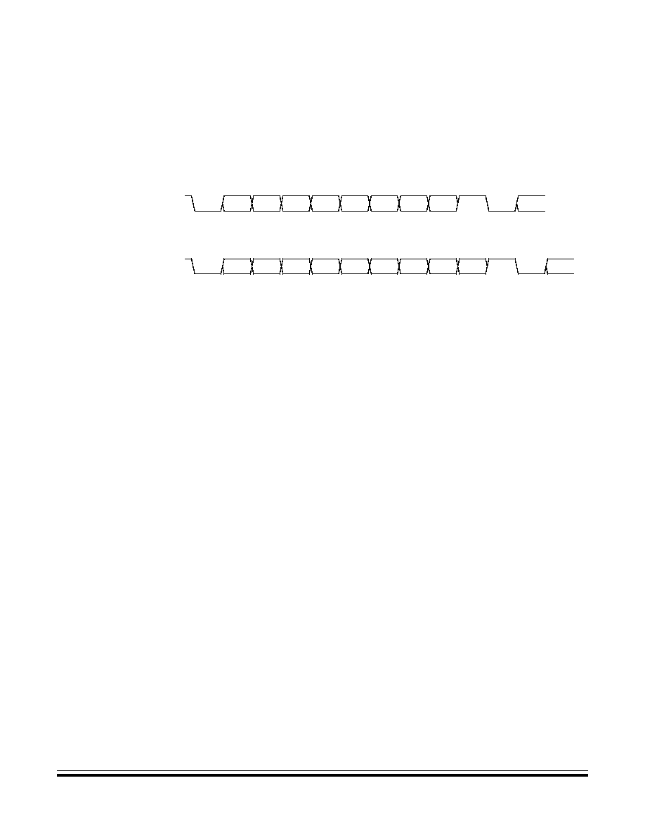
12.3.1 Data Format
The SCI uses the standard non-return-to-zero mark/space data format illustrated
in Figure 12-4.
Figure 12-4. SCI Data Formats
12.3.2 Transmitter
Figure 12-5 shows the structure of the SCI transmitter.
12.3.3 Character Length
The transmitter can accommodate either 8-bit or 9-bit data. The state of the M bit
in SCI control register 1 (SCC1) determines character length. When transmitting
9-bit data, bit T8 in SCI control register 3 (SCC3) is the ninth bit (bit 8).
12.3.4 Character Transmission
During an SCI transmission, the transmit shift register shifts a character out to the
PTE0/TxD pin. The SCI data register (SCDR) is the write-only buffer between the
internal data bus and the transmit shift register. To initiate an SCI transmission:
1.
Initialize the Tx and Rx rate in the SCI baud register (SCBR) ($0019) see
2.
Enable the SCI by writing a logic 1 to ENSCI in SCI control register 1 (SCC1)
($0013).
3.
Enable the transmitter by writing a logic 1 to the transmitter enable bit (TE)
in SCI control register 2 (SCC2) ($0014).
4.
Clear the SCI transmitter empty bit (SCTE) by first reading SCI status
register (SCS1) ($0016) and then writing to the SCDR ($0018).
5.
Repeat step 3 for each subsequent transmission.
At the start of a transmission, transmitter control logic automatically loads the
transmit shift register with a preamble of 10 or 11 logic 1s. After the preamble shifts
out, control logic transfers the SCDR data into the transmit shift register. A logic 0
start bit automatically goes into the least significant bit position of the transmit shift
register. A logic 1 stop bit goes into the most significant bit position.
BIT 5
START
BIT
BIT 0
BIT 1
NEXT
STOP
BIT
START
BIT
8-BIT DATA FORMAT
(BIT M IN SCC1 CLEAR)
START
BIT
BIT 0
NEXT
STOP
BIT
START
BIT
9-BIT DATA FORMAT
(BIT M IN SCC1 SET)
BIT 1
BIT 2
BIT 3
BIT 4
BIT 5
BIT 6
BIT 7
BIT 8
BIT 2
BIT 3
BIT 4
BIT 6
BIT 7
POSSIBLE
PARITY
BIT
POSSIBLE
PARITY
BIT
相關(guān)PDF資料 |
PDF描述 |
|---|---|
| MC68HC08AZ32CFU | 8-BIT, MROM, MICROCONTROLLER, PQFP64 |
| MC68HC08AZ48CFU | 8-BIT, MROM, 8.4 MHz, MICROCONTROLLER, PQFP64 |
| MC68HC08KH12FU | 8-BIT, MROM, 6 MHz, MICROCONTROLLER, PQFP64 |
| MC68HC08XL36CB | 8-BIT, MROM, 8.2 MHz, MICROCONTROLLER, PDIP56 |
| MC68HC11A0FNR2 | 8-BIT, MICROCONTROLLER, PQCC52 |
相關(guān)代理商/技術(shù)參數(shù) |
參數(shù)描述 |
|---|---|
| MC68HC08AZ0 | 制造商:MOTOROLA 制造商全稱:Motorola, Inc 功能描述:Advance Information |
| MC68HC08AZ0CFU | 制造商:MOTOROLA 制造商全稱:Motorola, Inc 功能描述:Advance Information |
| MC68HC08AZ16 | 制造商:MOTOROLA 制造商全稱:Motorola, Inc 功能描述:HCMOS Microcontroller Unit |
| MC68HC08AZ24 | 制造商:MOTOROLA 制造商全稱:Motorola, Inc 功能描述:HCMOS Microcontroller Unit |
| MC68HC08AZ32 | 制造商:FREESCALE 制造商全稱:Freescale Semiconductor, Inc 功能描述:Advance Information |
發(fā)布緊急采購,3分鐘左右您將得到回復(fù)。