- 您現(xiàn)在的位置:買賣IC網(wǎng) > PDF目錄45212 > MC68336GVFT20 (MOTOROLA INC) 32-BIT, 20.97 MHz, MICROCONTROLLER, PQFP16 PDF資料下載
參數(shù)資料
| 型號(hào): | MC68336GVFT20 |
| 廠商: | MOTOROLA INC |
| 元件分類: | 微控制器/微處理器 |
| 英文描述: | 32-BIT, 20.97 MHz, MICROCONTROLLER, PQFP16 |
| 封裝: | PLASTIC, QFP-160 |
| 文件頁(yè)數(shù): | 207/434頁(yè) |
| 文件大?。?/td> | 6093K |
| 代理商: | MC68336GVFT20 |
第1頁(yè)第2頁(yè)第3頁(yè)第4頁(yè)第5頁(yè)第6頁(yè)第7頁(yè)第8頁(yè)第9頁(yè)第10頁(yè)第11頁(yè)第12頁(yè)第13頁(yè)第14頁(yè)第15頁(yè)第16頁(yè)第17頁(yè)第18頁(yè)第19頁(yè)第20頁(yè)第21頁(yè)第22頁(yè)第23頁(yè)第24頁(yè)第25頁(yè)第26頁(yè)第27頁(yè)第28頁(yè)第29頁(yè)第30頁(yè)第31頁(yè)第32頁(yè)第33頁(yè)第34頁(yè)第35頁(yè)第36頁(yè)第37頁(yè)第38頁(yè)第39頁(yè)第40頁(yè)第41頁(yè)第42頁(yè)第43頁(yè)第44頁(yè)第45頁(yè)第46頁(yè)第47頁(yè)第48頁(yè)第49頁(yè)第50頁(yè)第51頁(yè)第52頁(yè)第53頁(yè)第54頁(yè)第55頁(yè)第56頁(yè)第57頁(yè)第58頁(yè)第59頁(yè)第60頁(yè)第61頁(yè)第62頁(yè)第63頁(yè)第64頁(yè)第65頁(yè)第66頁(yè)第67頁(yè)第68頁(yè)第69頁(yè)第70頁(yè)第71頁(yè)第72頁(yè)第73頁(yè)第74頁(yè)第75頁(yè)第76頁(yè)第77頁(yè)第78頁(yè)第79頁(yè)第80頁(yè)第81頁(yè)第82頁(yè)第83頁(yè)第84頁(yè)第85頁(yè)第86頁(yè)第87頁(yè)第88頁(yè)第89頁(yè)第90頁(yè)第91頁(yè)第92頁(yè)第93頁(yè)第94頁(yè)第95頁(yè)第96頁(yè)第97頁(yè)第98頁(yè)第99頁(yè)第100頁(yè)第101頁(yè)第102頁(yè)第103頁(yè)第104頁(yè)第105頁(yè)第106頁(yè)第107頁(yè)第108頁(yè)第109頁(yè)第110頁(yè)第111頁(yè)第112頁(yè)第113頁(yè)第114頁(yè)第115頁(yè)第116頁(yè)第117頁(yè)第118頁(yè)第119頁(yè)第120頁(yè)第121頁(yè)第122頁(yè)第123頁(yè)第124頁(yè)第125頁(yè)第126頁(yè)第127頁(yè)第128頁(yè)第129頁(yè)第130頁(yè)第131頁(yè)第132頁(yè)第133頁(yè)第134頁(yè)第135頁(yè)第136頁(yè)第137頁(yè)第138頁(yè)第139頁(yè)第140頁(yè)第141頁(yè)第142頁(yè)第143頁(yè)第144頁(yè)第145頁(yè)第146頁(yè)第147頁(yè)第148頁(yè)第149頁(yè)第150頁(yè)第151頁(yè)第152頁(yè)第153頁(yè)第154頁(yè)第155頁(yè)第156頁(yè)第157頁(yè)第158頁(yè)第159頁(yè)第160頁(yè)第161頁(yè)第162頁(yè)第163頁(yè)第164頁(yè)第165頁(yè)第166頁(yè)第167頁(yè)第168頁(yè)第169頁(yè)第170頁(yè)第171頁(yè)第172頁(yè)第173頁(yè)第174頁(yè)第175頁(yè)第176頁(yè)第177頁(yè)第178頁(yè)第179頁(yè)第180頁(yè)第181頁(yè)第182頁(yè)第183頁(yè)第184頁(yè)第185頁(yè)第186頁(yè)第187頁(yè)第188頁(yè)第189頁(yè)第190頁(yè)第191頁(yè)第192頁(yè)第193頁(yè)第194頁(yè)第195頁(yè)第196頁(yè)第197頁(yè)第198頁(yè)第199頁(yè)第200頁(yè)第201頁(yè)第202頁(yè)第203頁(yè)第204頁(yè)第205頁(yè)第206頁(yè)當(dāng)前第207頁(yè)第208頁(yè)第209頁(yè)第210頁(yè)第211頁(yè)第212頁(yè)第213頁(yè)第214頁(yè)第215頁(yè)第216頁(yè)第217頁(yè)第218頁(yè)第219頁(yè)第220頁(yè)第221頁(yè)第222頁(yè)第223頁(yè)第224頁(yè)第225頁(yè)第226頁(yè)第227頁(yè)第228頁(yè)第229頁(yè)第230頁(yè)第231頁(yè)第232頁(yè)第233頁(yè)第234頁(yè)第235頁(yè)第236頁(yè)第237頁(yè)第238頁(yè)第239頁(yè)第240頁(yè)第241頁(yè)第242頁(yè)第243頁(yè)第244頁(yè)第245頁(yè)第246頁(yè)第247頁(yè)第248頁(yè)第249頁(yè)第250頁(yè)第251頁(yè)第252頁(yè)第253頁(yè)第254頁(yè)第255頁(yè)第256頁(yè)第257頁(yè)第258頁(yè)第259頁(yè)第260頁(yè)第261頁(yè)第262頁(yè)第263頁(yè)第264頁(yè)第265頁(yè)第266頁(yè)第267頁(yè)第268頁(yè)第269頁(yè)第270頁(yè)第271頁(yè)第272頁(yè)第273頁(yè)第274頁(yè)第275頁(yè)第276頁(yè)第277頁(yè)第278頁(yè)第279頁(yè)第280頁(yè)第281頁(yè)第282頁(yè)第283頁(yè)第284頁(yè)第285頁(yè)第286頁(yè)第287頁(yè)第288頁(yè)第289頁(yè)第290頁(yè)第291頁(yè)第292頁(yè)第293頁(yè)第294頁(yè)第295頁(yè)第296頁(yè)第297頁(yè)第298頁(yè)第299頁(yè)第300頁(yè)第301頁(yè)第302頁(yè)第303頁(yè)第304頁(yè)第305頁(yè)第306頁(yè)第307頁(yè)第308頁(yè)第309頁(yè)第310頁(yè)第311頁(yè)第312頁(yè)第313頁(yè)第314頁(yè)第315頁(yè)第316頁(yè)第317頁(yè)第318頁(yè)第319頁(yè)第320頁(yè)第321頁(yè)第322頁(yè)第323頁(yè)第324頁(yè)第325頁(yè)第326頁(yè)第327頁(yè)第328頁(yè)第329頁(yè)第330頁(yè)第331頁(yè)第332頁(yè)第333頁(yè)第334頁(yè)第335頁(yè)第336頁(yè)第337頁(yè)第338頁(yè)第339頁(yè)第340頁(yè)第341頁(yè)第342頁(yè)第343頁(yè)第344頁(yè)第345頁(yè)第346頁(yè)第347頁(yè)第348頁(yè)第349頁(yè)第350頁(yè)第351頁(yè)第352頁(yè)第353頁(yè)第354頁(yè)第355頁(yè)第356頁(yè)第357頁(yè)第358頁(yè)第359頁(yè)第360頁(yè)第361頁(yè)第362頁(yè)第363頁(yè)第364頁(yè)第365頁(yè)第366頁(yè)第367頁(yè)第368頁(yè)第369頁(yè)第370頁(yè)第371頁(yè)第372頁(yè)第373頁(yè)第374頁(yè)第375頁(yè)第376頁(yè)第377頁(yè)第378頁(yè)第379頁(yè)第380頁(yè)第381頁(yè)第382頁(yè)第383頁(yè)第384頁(yè)第385頁(yè)第386頁(yè)第387頁(yè)第388頁(yè)第389頁(yè)第390頁(yè)第391頁(yè)第392頁(yè)第393頁(yè)第394頁(yè)第395頁(yè)第396頁(yè)第397頁(yè)第398頁(yè)第399頁(yè)第400頁(yè)第401頁(yè)第402頁(yè)第403頁(yè)第404頁(yè)第405頁(yè)第406頁(yè)第407頁(yè)第408頁(yè)第409頁(yè)第410頁(yè)第411頁(yè)第412頁(yè)第413頁(yè)第414頁(yè)第415頁(yè)第416頁(yè)第417頁(yè)第418頁(yè)第419頁(yè)第420頁(yè)第421頁(yè)第422頁(yè)第423頁(yè)第424頁(yè)第425頁(yè)第426頁(yè)第427頁(yè)第428頁(yè)第429頁(yè)第430頁(yè)第431頁(yè)第432頁(yè)第433頁(yè)第434頁(yè)
MC68336/376
ELECTRICAL CHARACTERISTICS
MOTOROLA
USER’S MANUAL
A-9
NOTES:
1. All AC timing is shown with respect to 20% VDD and 70% VDD levels unless otherwise noted.
2. The base configuration of the MC68336/376 requires a 20.97 MHz crystal reference.
3. When an external clock is used, minimum high and low times are based on a 50% duty cycle. The minimum
allowable tXcyc period is reduced when the duty cycle of the external clock signal varies. The relationship between
external clock input duty cycle and minimum tXcyc is expressed:
Minimum tXcyc period = minimum tXCHL / (50% –external clock input duty cycle tolerance).
4. Parameters for an external clock signal applied while the internal PLL is disabled (MODCLK pin held low during
reset). Does not pertain to an external VCO reference applied while the PLL is enabled (MODCLK pin held high
during reset). When the PLL is enabled, the clock synthesizer detects successive transitions of the reference
signal. If transitions occur within the correct clock period, rise/fall times and duty cycle are not critical.
5. Address access time = (2.5 + WS) tcyc – tCHAV – tDICL
Chip select access time = (2 + WS) tcyc – tLSA – tDICL
Where: WS = number of wait states. When fast termination is used (2 clock bus) WS = –1.
6. Specification 9A is the worst-case skew between AS and DS or CS. The amount of skew depends on the relative
loading of these signals. When loads are kept within specified limits, skew will not cause AS and DS to fall outside
the limits shown in specification 9.
7. If multiple chip selects are used, CS width negated (specification 15) applies to the time from the negation of a
heavily loaded chip select to the assertion of a lightly loaded chip select. The CS width negated specification
between multiple chip selects does not apply to chip selects being used for synchronous ECLK cycles.
8. Hold times are specified with respect to DS or CS on asynchronous reads and with respect to CLKOUT on fast
cycle reads. The user is free to use either hold time.
9. Maximum value is equal to (tcyc / 2) + 25 ns.
10. If the asynchronous setup time (specification 47A) requirements are satisfied, the DSACK[1:0] low to data setup
time (specification 31) and DSACK[1:0] low to BERR low setup time (specification 48) can be ignored. The data
must only satisfy the data-in to clock low setup time (specification 27) for the following clock cycle. BERR must
satisfy only the late BERR low to clock low setup time (specification 27A) for the following clock cycle.
11. To ensure coherency during every operand transfer, BG will not be asserted in response to BR until after all
cycles of the current operand transfer are complete and RMC is negated.
12. In the absence of DSACK[1:0], BERR is an asynchronous input using the asynchronous setup time (specification
47A).
13. After external RESET negation is detected, a short transition period (approximately 2 tcyc) elapses, then the SIM
drives RESET low for 512 tcyc.
14. External assertion of the RESET input can overlap internally-generated resets. To insure that an external
reset is recognized in all cases, RESET must be asserted for at least 590 CLKOUT cycles.
15. External logic must pull RESET high during this period in order for normal MCU operation to begin.
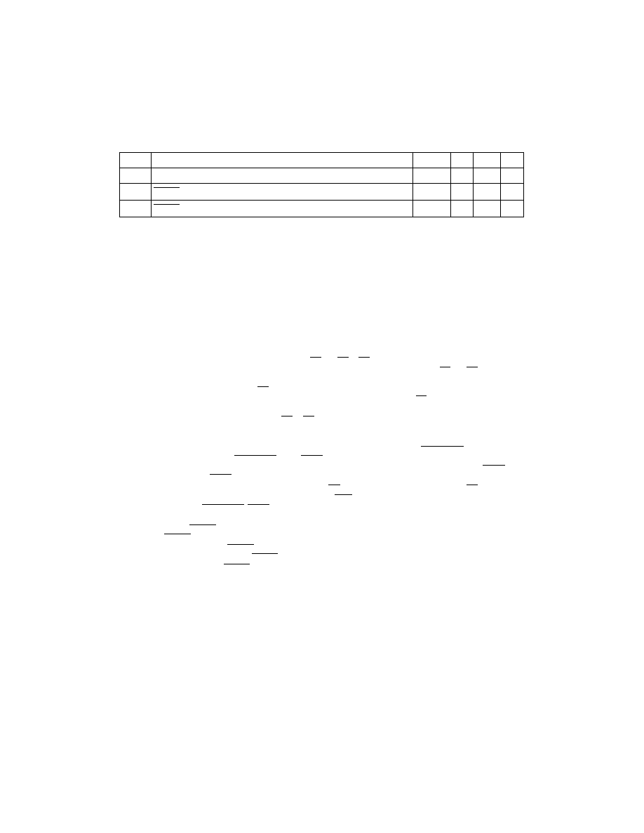
76
Mode Select Hold Time
tMSH
0—
ns
77
RESET Assertion Time13
tRSTA
4—
tcyc
78
RESET Rise Time14, 15
tRSTR
—10
tcyc
Table A-6 AC Timing (Continued)
(VDD and VDDSYN = 5.0 Vdc ±5%, VSS = 0 Vdc, TA = TL to TH)
1
Num
Characteristic
Symbol
Min
Max
Unit
336376UMBook Page 9 Friday, November 15, 1996 2:09 PM
相關(guān)PDF資料 |
PDF描述 |
|---|---|
| MC68336ACFT20B1 | 32-BIT, 20.97 MHz, MICROCONTROLLER, PQFP16 |
| MC68376BGVFT20 | 32-BIT, MROM, 20.97 MHz, MICROCONTROLLER, PQFP16 |
| MC68340FE16C | 32-BIT, 16.78 MHz, MICROCONTROLLER, CQFP144 |
| MC68340RP16E | 32-BIT, 16.78 MHz, MICROCONTROLLER, PPGA145 |
| MC68340RP16 | 32-BIT, 16.78 MHz, MICROCONTROLLER, PPGA145 |
相關(guān)代理商/技術(shù)參數(shù) |
參數(shù)描述 |
|---|---|
| MC68340 | 制造商:FREESCALE 制造商全稱:Freescale Semiconductor, Inc 功能描述:Integrated Processor with DMA User’s Manual |
| MC68340AB16E | 功能描述:微處理器 - MPU 32BIT MPU DMA TIMER RoHS:否 制造商:Atmel 處理器系列:SAMA5D31 核心:ARM Cortex A5 數(shù)據(jù)總線寬度:32 bit 最大時(shí)鐘頻率:536 MHz 程序存儲(chǔ)器大小:32 KB 數(shù)據(jù) RAM 大小:128 KB 接口類型:CAN, Ethernet, LIN, SPI,TWI, UART, USB 工作電源電壓:1.8 V to 3.3 V 最大工作溫度:+ 85 C 安裝風(fēng)格:SMD/SMT 封裝 / 箱體:FBGA-324 |
| MC68340AB16E | 制造商:Freescale Semiconductor 功能描述:Microprocessor |
| MC68340AB16EB1 | 制造商:Rochester Electronics LLC 功能描述: 制造商:Freescale Semiconductor 功能描述: |
| MC68340AB25E | 功能描述:微處理器 - MPU 25MHz 4.8MIPS RoHS:否 制造商:Atmel 處理器系列:SAMA5D31 核心:ARM Cortex A5 數(shù)據(jù)總線寬度:32 bit 最大時(shí)鐘頻率:536 MHz 程序存儲(chǔ)器大小:32 KB 數(shù)據(jù) RAM 大小:128 KB 接口類型:CAN, Ethernet, LIN, SPI,TWI, UART, USB 工作電源電壓:1.8 V to 3.3 V 最大工作溫度:+ 85 C 安裝風(fēng)格:SMD/SMT 封裝 / 箱體:FBGA-324 |
發(fā)布緊急采購(gòu),3分鐘左右您將得到回復(fù)。