- 您現(xiàn)在的位置:買賣IC網(wǎng) > PDF目錄67965 > MC68307FG (MOTOROLA INC) 32-BIT, MICROCONTROLLER, PQFP100 PDF資料下載
參數(shù)資料
| 型號: | MC68307FG |
| 廠商: | MOTOROLA INC |
| 元件分類: | 微控制器/微處理器 |
| 英文描述: | 32-BIT, MICROCONTROLLER, PQFP100 |
| 封裝: | PLASTIC, QFP-100 |
| 文件頁數(shù): | 11/34頁 |
| 文件大?。?/td> | 354K |
| 代理商: | MC68307FG |
第1頁第2頁第3頁第4頁第5頁第6頁第7頁第8頁第9頁第10頁當(dāng)前第11頁第12頁第13頁第14頁第15頁第16頁第17頁第18頁第19頁第20頁第21頁第22頁第23頁第24頁第25頁第26頁第27頁第28頁第29頁第30頁第31頁第32頁第33頁第34頁
MOTOROLA
MC68307 TECHNICAL INFORMATION
19
ELECTRICAL CHARACTERISTICS
AC ELECTRICAL SPECIFICATION DEFINITIONS
The AC specications presented consist of output delays, input setup and hold times and signal skew times. All
signals are specied relative to an appropriate edge of the clock and possibly to one or more other signals.
The measurement of the AC specications is dened by the waveforms shown in Figure 6. To test the parameters
guaranteed by Motorola, inputs must be driven to the voltage levels specied in the gure. Outputs are specied
with minimum and/or maximum limits, as appropriate, and are measured as shown. Inputs are specied with
minimum setup and hold times, and are measured as shown. Finally, the measurement for signal-to-signal
specications are shown.
Note that the testing levels used to verify conformance to the AC specications does not affect the guaranteed
DC operation of the device as specied in the DC electrical characteristics.
a. Not including internal pull-up or pull-down.
b. Currents listed are with no loading.
c. Capacitance is periodically sampled rather than 100% tested.
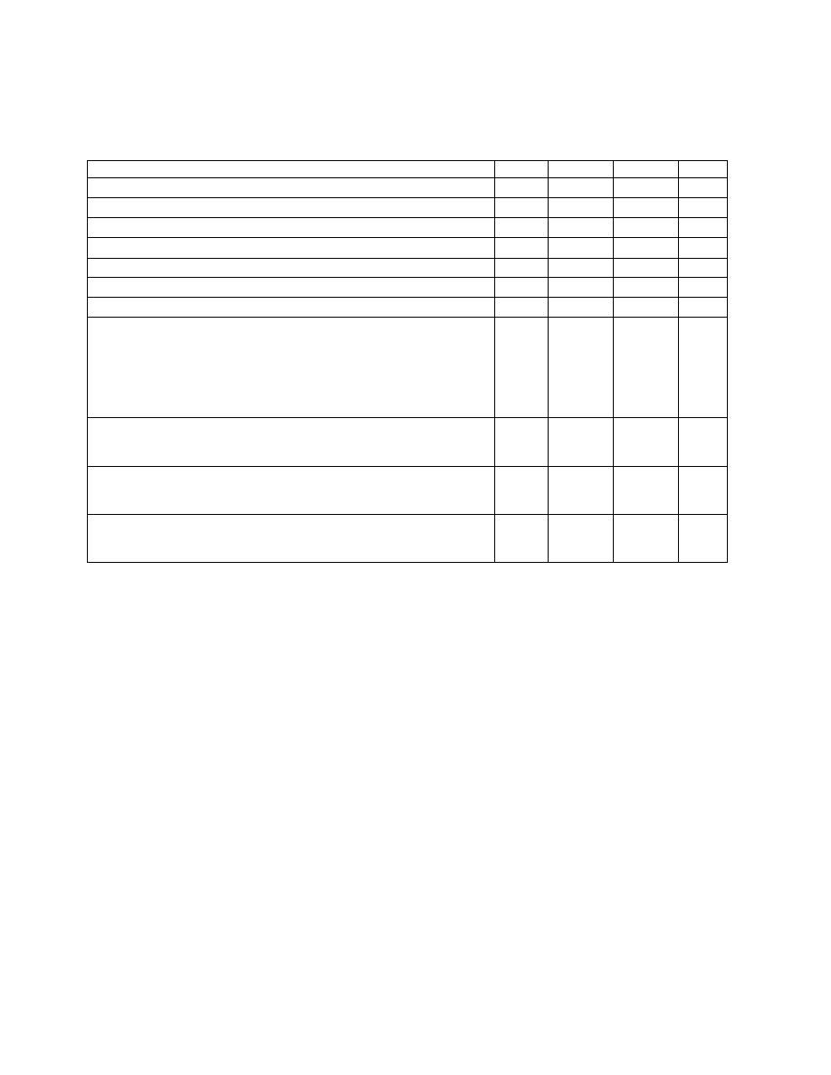
PRELIMINARY DC ELECTRICAL SPECIFICATIONS
Characteristic
Symbol
Min
Max
Unit
Input high voltage (except clock)
VIH
2.0
VCC
V
Input low voltage
VIL
GND
0.8
V
Clock input high voltage
VIHC
0.7 VCC
VCC + 0.3
V
Input leakage current @5.25V (all input-only pins)a
IIN
– 2.5
2.5
A
Three-state (off state) input current @2.4V/0.4V
ITSI
—20
A
Output high voltage (IOH = rated maximum)
VOH
VCC – 0.75
—
V
Output low voltage (IOL = rated maximum)
VOL
—
0.5
V
Current dissipation
VCC = 5.0V±0.5V
b
fEXT = 16.67MHz
VCC = 3.3V±0.3V
b
fEXT = 8MHz
Low power STOP mode
VCC = 5.0V±0.5V
fEXT = 16.67MHz
VCC = 3.3V±0.3V
fEXT = 8MHz
ID
—
30
TBD
mA
Power dissipation
VCC = 5.0V±0.5V
fEXT = 16.67MHz
VCC = 3.3V±0.3V
fEXT = 8MHz
PD
—
0.26
TBD
W
Input capacitancec
All input-only pins
All I/O pins
CIN
—
10
20
pF
Load capacitancec
All output pins (except SCL and SDA)
SCL, SDA
CL
—
100
400
pF
相關(guān)PDF資料 |
PDF描述 |
|---|---|
| MC68322FT25 | 32-BIT, 25 MHz, RISC PROCESSOR, PQFP160 |
| MC68322FT20 | 32-BIT, 20 MHz, RISC PROCESSOR, PQFP160 |
| MC68322FT16 | 32-BIT, 16.667 MHz, RISC PROCESSOR, PQFP160 |
| MC68330FC16 | 32-BIT, 16.78 MHz, MICROPROCESSOR, PQFP132 |
| MC68332AMPV16 | 32-BIT, 16.78 MHz, MICROCONTROLLER, PQFP144 |
相關(guān)代理商/技術(shù)參數(shù) |
參數(shù)描述 |
|---|---|
| MC68307UM | 制造商:MOTOROLA 制造商全稱:Motorola, Inc 功能描述:Technical Summary Integrated Multiple-Bus Processor |
| MC68307V | 制造商:MOTOROLA 制造商全稱:Motorola, Inc 功能描述:Technical Summary Integrated Multiple-Bus Processor |
| MC68322 | 制造商:MOTOROLA 制造商全稱:Motorola, Inc 功能描述:Integrated Printer Processor |
| MC68322AD | 制造商:MOTOROLA 制造商全稱:Motorola, Inc 功能描述:Integrated Printer Processor |
| MC68322FT20 | 制造商:Rochester Electronics LLC 功能描述:- Bulk |
發(fā)布緊急采購,3分鐘左右您將得到回復(fù)。
