- 您現(xiàn)在的位置:買賣IC網(wǎng) > PDF目錄369896 > MC14034B (Motorola, Inc.) 8-Bit Universal Bus Register PDF資料下載
參數(shù)資料
| 型號: | MC14034B |
| 廠商: | Motorola, Inc. |
| 英文描述: | 8-Bit Universal Bus Register |
| 中文描述: | 8位通用總線注冊 |
| 文件頁數(shù): | 4/9頁 |
| 文件大?。?/td> | 313K |
| 代理商: | MC14034B |

MOTOROLA CMOS LOGIC DATA
MC14034B
138
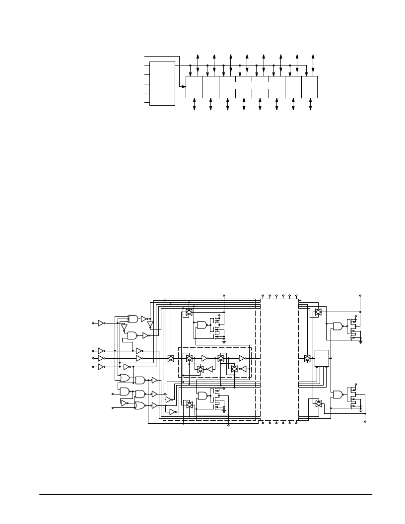
EXPANDED BLOCK DIAGRAM
SERIAL DATA INPUT
PARALLEL/SERIAL P/S
A/B
ENABLE A
ASYN/SYN A/S
CLOCK
CONTROL
LOGIC
A1
A2
A3
A4
A5
A6
A7
A8
B1
B2
B3
B4
B5
B6
B7
B8
DATA
DATA
8–BIT REGISTER
OPERATING CHARACTERISTICS
The MC14034B is composed of eight register cells con-
nected in cascade with additional control logic. Each register
cell is composed of one “D” master–slave flip–flop with sepa-
rate internal clocks, and two data transfer gates allowing the
data to be transferred bi–directionally from bus A to bus B
and from bus B to bus A, and to be memorized. Besides the
single phase clock and the serial data inputs, the control log-
ic provides four other features:
A Enable Input —
When high, this input enables the bus A
data lines.
A/B Input (Data A or B) —
This input controls the direc-
tion of data flow: when high, the data flows from bus A to bus
B; when low, the data flows from bus B to bus A.
P/S Input (Parallel/Serial) —
This input controls the data
input mode (parallel or serial). When high, the data is trans-
ferred to the register in a parallel asynchronous mode or a
parallel synchronous mode (positive clock transition). When
low, the data is entered into the register in a serial synchro-
nous mode (positive clock transition).
A/S Input (Asynchronous/Synchronous to the Clock)
—
When this input is high, the data is transferred indepen-
dently from the clock rate; when low, the clock is enabled and
the data is transferred synchronously.
LOGIC DIAGRAM
A ENABLE
9
A/B 11
SERIAL DATA 10
PARALLEL SERIAL 13
ASYN/SYN 14
CLOCK 15
CM
*D FLIP FLOP
VDD
CS
VDD
A1
16
A2
17
A3
18
A4
19
A5
20
A6
21
A7
22
A8
23
VDD
6 STAGES
(SAME AS
STAGE 1)
*D
FLIP–
FLOP
D
CMCS
Q
8
B1
7
B2
6
B3
5
B4
4
B5
3
B6
2
B7
1
B8
相關(guān)PDF資料 |
PDF描述 |
|---|---|
| MC14034 | 8-Bit Universal Bus Register |
| MC14035B | 4-Bit Parallel-In/Parallel-Out Shift Register |
| MC14040BCL | ExpressCard Single Power Interface Switch 20-TSSOP -40 to 85 |
| MC14040 | ExpressCard Single Power Interface Switch 24-HTSSOP -40 to 85 |
| MC14040BCP | ExpressCard Single Power Interface Switch 20-TSSOP -40 to 85 |
相關(guān)代理商/技術(shù)參數(shù) |
參數(shù)描述 |
|---|---|
| MC14035B | 制造商:MOTOROLA 制造商全稱:Motorola, Inc 功能描述:4-Bit Parallel-In/Parallel-Out Shift Register |
| MC14035BCL | 制造商:Motorola Inc 功能描述: |
| MC14035BCLD | 制造商:Motorola 功能描述:MOTOROLA NXC7B |
| MC14035BCP | 制造商:Rochester Electronics LLC 功能描述:- Bulk |
| MC14035BCPD | 制造商:n/a 功能描述:14035 MOT'82 LOC: SB-178 |
發(fā)布緊急采購,3分鐘左右您將得到回復(fù)。