- 您現(xiàn)在的位置:買賣IC網(wǎng) > PDF目錄371004 > MC10H115L (MOTOROLA INC) 8 MEGABIT 3.3 VOLT SERIAL CONFIGURATION - NOT RECOMMENDED for NEW DESIGN PDF資料下載
參數(shù)資料
| 型號: | MC10H115L |
| 廠商: | MOTOROLA INC |
| 元件分類: | 通用總線功能 |
| 英文描述: | 8 MEGABIT 3.3 VOLT SERIAL CONFIGURATION - NOT RECOMMENDED for NEW DESIGN |
| 中文描述: | LINE RECEIVER, CDIP16 |
| 封裝: | CERAMIC, DIP-16 |
| 文件頁數(shù): | 1/3頁 |
| 文件大小: | 96K |
| 代理商: | MC10H115L |

SEMICONDUCTOR TECHNICAL DATA
2–216
REV 5
Motorola, Inc. 1996
3/93
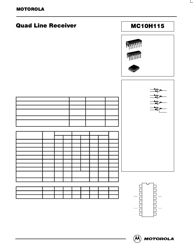
The MC10H115 is a quad differential amplifier designed for use in sensing
differential signals over long lines. This 10H part is a functional/ pinout
duplication of the standard MECL 10K family part, with 100% improvement in
counting frequency and no increase in power–supply current.
The base bias supply (VBB) is made available at Pin 9 to make the device
useful as a Schmitt trigger, or in other applications where a stable reference
voltage is necessary. Active current sources provide the MC10H115 with
excellent common mode rejection. If any amplifier in a package is not used, one
input of that amplifier must be connected to VBB (Pin 9) to prevent upsetting the
current source bias network.
Propagation Delay, 1.0 ns Typical
Power Dissipation 110 mW Typ/Pkg (No Load)
Improved Noise Margin 150 mV (Over Operating Voltage and
Temperature Range)
Voltage Compensated
MECL 10K–Compatible
MAXIMUM RATINGS
Characteristic
Symbol
Rating
Unit
Power Supply (VCC = 0)
Input Voltage (VCC = 0)
Output Current — Continuous
VEE
VI
Iout
–8.0 to 0
Vdc
0 to VEE
50
100
Vdc
— Surge
mA
Operating Temperature Range
TA
Tstg
0 to +75
°
C
Storage Temperature Range — Plastic
— Ceramic
–55 to +150
–55 to +165
°
C
°
C
ELECTRICAL CHARACTERISTICS
(VEE = –5.2 V
±
5%) (2)
0
°
25
°
75
°
Characteristic
Symbol
Min
Max
Min
Max
Min
Max
Unit
Power Supply Current
IE
IinH
ICBO
VBB
VOH
VOL
VIH
VIL
VCMR
—
29
—
26
—
29
mA
Input Current High
—
150
—
95
—
95
μ
A
μ
A
Input Leakage Current
—
1.5
—
1.0
—
1.0
Reference Voltage
–1.38
–1.27
–1.35
–1.25
–1.31
–1.19
Vdc
High Output Voltage
–1.02
–0.84
–0.98
–0.81
–0.92
–0.735
Vdc
Low Output Voltage
–1.95
–1.63
–1.95
–1.63
–1.95
–1.60
Vdc
High Input Voltage (1)
–1.17
–0.84
–1.13
–0.81
–1.07
–0.735
Vdc
Low Input Voltage (1)
–1.95
–1.48
–1.95
–1.48
–1.95
–1.45
Vdc
Common Mode
Range (3)
—
—
–2.85 to –0.8
—
—
Vdc
Input Sensitivity (4)
VPP
—
—
150 typ
—
—
mVPP
AC PARAMETERS
Propagation Delay
tpd
tr
tf
0.4
1.3
0.4
1.3
0.45
1.45
ns
Rise Time
0.5
1.4
0.5
1.5
0.5
1.6
ns
Fall Time
0.5
1.4
0.5
1.5
0.5
1.6
ns
NOTES:
1. When VBB is used as the reference voltage.
equilibrium has been established. The circuit is in a test socket or mounted on a printed circuit board and transverse
air flow greater than 500 linear fpm is maintained. Outputs are terminated through a 50–ohm resistor to –2.0 volts.
3. Differential input not to exceed 1.0 Vdc.
4. 150 mVp–p differential input required to obtain full logic swing on output.
LOGIC DIAGRAM
DIP
PIN ASSIGNMENT
VCC1
AOUT
BOUT
AIN
AIN
BIN
BIN
VEE
VCC2
DOUT
COUT
DIN
DIN
CIN
CIN
VBB
16
15
14
13
12
11
10
9
1
2
3
4
5
6
7
8
2
5
4
3
6
7
14
11
10
15
12
13
9
*and bypassed (when used) with 0.01
μ
F to 0.1
μ
F
The MC10H115 is designed to be used in sensing
differential signals over long lines. The bias supply
(VBB) is made available to make the device useful as a
reference voltage is necessary.
Active current sources provide these receivers with
excellent common–mode noise rejection. If any
amplifier in a package is not used, one input of that
amplifier must be connected to VBB to prevent
The MC10H115 does not have internal–input pull–
down resistors. This provides high impedance to the
amplifier input and facilitates differential connections.
Applications:
Low Level Receiver
Schmitt Trigger
Voltage Level
Interface
VBB*
When input pin with
bubble goes positive
its respective output
pin with bubble goes
positive.
VCC1 = Pin 1
VCC2 = Pin 16
VEE = Pin 8
L SUFFIX
CERAMIC PACKAGE
CASE 620–10
P SUFFIX
PLASTIC PACKAGE
CASE 648–08
FN SUFFIX
PLCC
CASE 775–02
Pin assignment is for Dual–in–Line Package.
For PLCC pin assignment, see the Pin Conversion
Tables on page 6–11 of the Motorola MECL Data
Book (DL122/D).
相關(guān)PDF資料 |
PDF描述 |
|---|---|
| MC10H115P | 8 MEGABIT 3.3 VOLT SERIAL CONFIGURATION - NOT RECOMMENDED for NEW DESIGN |
| MC10H116D | 8 MEGABIT 3.3 VOLT SERIAL CONFIGURATION - NOT RECOMMENDED for NEW DESIGN |
| MC10H116 | Triple Line Receiver |
| MC10H116FN | Triple Line Receiver |
| MC10H116L | 16 MEGABIT 3.3 VOLT SERIAL CONFIGURATION - NOT RECOMMENDED for NEW DESIGN |
相關(guān)代理商/技術(shù)參數(shù) |
參數(shù)描述 |
|---|---|
| MC10H115M | 功能描述:總線接收器 Quad Diff Amplifier RoHS:否 制造商:Texas Instruments 接收機(jī)數(shù)量:4 接收機(jī)信號類型:Differential 接口類型:EIA/TIA-422-B, V.11 工作電源電壓:3.3 V 最大工作溫度:+ 85 C 最小工作溫度:- 40 C 封裝 / 箱體:TSSOP-16 封裝:Reel |
| MC10H115MEL | 功能描述:總線接收器 Quad Diff Amplifier RoHS:否 制造商:Texas Instruments 接收機(jī)數(shù)量:4 接收機(jī)信號類型:Differential 接口類型:EIA/TIA-422-B, V.11 工作電源電壓:3.3 V 最大工作溫度:+ 85 C 最小工作溫度:- 40 C 封裝 / 箱體:TSSOP-16 封裝:Reel |
| MC10H115MELG | 功能描述:總線接收器 Quad Diff Amplifier RoHS:否 制造商:Texas Instruments 接收機(jī)數(shù)量:4 接收機(jī)信號類型:Differential 接口類型:EIA/TIA-422-B, V.11 工作電源電壓:3.3 V 最大工作溫度:+ 85 C 最小工作溫度:- 40 C 封裝 / 箱體:TSSOP-16 封裝:Reel |
| MC10H115MG | 功能描述:總線接收器 Quad Diff Amplifier RoHS:否 制造商:Texas Instruments 接收機(jī)數(shù)量:4 接收機(jī)信號類型:Differential 接口類型:EIA/TIA-422-B, V.11 工作電源電壓:3.3 V 最大工作溫度:+ 85 C 最小工作溫度:- 40 C 封裝 / 箱體:TSSOP-16 封裝:Reel |
| MC10H115ML | 制造商:Motorola Inc 功能描述: |
發(fā)布緊急采購,3分鐘左右您將得到回復(fù)。