- 您現(xiàn)在的位置:買賣IC網(wǎng) > PDF目錄379301 > MC100E195FN (MOTOROLA INC) PROGRAMMABLE DELAY CHIP PDF資料下載
參數(shù)資料
| 型號: | MC100E195FN |
| 廠商: | MOTOROLA INC |
| 元件分類: | 通用總線功能 |
| 英文描述: | PROGRAMMABLE DELAY CHIP |
| 中文描述: | ACTIVE DELAY LINE, COMPLEMENTARY OUTPUT, PQCC28 |
| 封裝: | PLASTIC, LCC-28 |
| 文件頁數(shù): | 1/5頁 |
| 文件大?。?/td> | 127K |
| 代理商: | MC100E195FN |
SEMICONDUCTOR TECHNICAL DATA
2–1
REV 2
Motorola, Inc. 1996
12/93
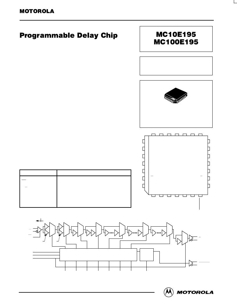
The MC10E/100E195 is a programmable delay chip (PDC) designed
primarily for clock de-skewing and timing adjustment. It provides variable
delay of a differential ECL input transition.
The delay section consists of a chain of gates organized as shown in
the logic symbol. The first two delay elements feature gates that have
been modified to have delays 1.25 and 1.5 times the basic gate delay of
approximately 80 ps. These two elements provide the E195 with a
digitally-selectable resolution of approximately 20 ps. The required
device delay is selected by the seven address inputs D[0:6], which are
latched on chip by a high signal on the latch enable (LEN) control.
Because the delay programmability of the E195 is achieved by purely
differential ECL gate delays the device will operate at frequencies of >1.0
GHz while maintaining over 600 mV of output swing.
The E195 thus offers very fine resolution, at very high frequencies, that
is selectable entirely from a digital input allowing for very accurate system
clock timing.
An eighth latched input, D7, is provided for cascading multiple PDC’s
for increased programmable range. The cascade logic allows full control
of multiple PDC’s, at the expense of only a single added line to the data
bus for each additional PDC, without the need for any external gating.
2.0ns Worst Case Delay Range
≈
20ps/Delay Step Resolution
>1.0GHz Bandwidth
On Chip Cascade Circuitry
Extended 100E VEE Range of –4.2 to –5.46V
75K
Input Pulldown Resistors
PIN NAMES
Pin
Function
IN/IN
EN
D[0:7]
Q/Q
LEN
SET MIN
SET MAX
CASCADE
Signal Input
Input Enable
Mux Select Inputs
Signal Output
Latch Enable
Min Delay Set
Max Delay Set
Cascade Signal
1
1
LOGIC DIAGRAM – SIMPLIFIED
VBB
IN
IN
EN
LEN
SET MIN
SET MAX
1
0
1
0
1
0
1
0
1
0
1
0
1
0
1
1
1
1
0
1
Q
Q
CASCADE
CASCADE
CASCADE
7 BIT LATCH
LEN
Q
LATCH
D
4 GATES
8 GATES
16 GATES
* 1.25
* 1.5
D0
D1
D2
D3
D4
D5
D6
D7
* DELAYS ARE 25% OR 50% LONGER THAN
*
STANDARD (STANDARD
≈
80 PS)
PROGRAMMABLE
DELAY CHIP
FN SUFFIX
PLASTIC PACKAGE
CASE 776-02
D2
D3
D4
D5
D6
D7
NC
NC
NC
EN
S
S
C
C
NC
NC
VCC
VCCO
Q
Q
VCCO
D1
D0
LEN
VEE
IN
IN
VBB
25
24
23
22
21
20
19
26
27
28
1
2
3
4
18
17
16
15
14
13
12
5
6
7
8
9
10
11
Pinout:
28-Lead PLCC
(Top View)
相關(guān)PDF資料 |
PDF描述 |
|---|---|
| MC10E196FN | PROGRAMMABLE DELAY CHIP |
| MC10E196 | PROGRAMMABLE DELAY CHIP |
| MC100E196FN | PROGRAMMABLE DELAY CHIP |
| MC10E404FN | QUAD DIFFERENTIAL AND/NAND |
| MC10E404 | QUAD DIFFERENTIAL AND/NAND |
相關(guān)代理商/技術(shù)參數(shù) |
參數(shù)描述 |
|---|---|
| MC100E195FNG | 功能描述:延遲線/計時元素 5V ECL Programmable Delay RoHS:否 制造商:Micrel 功能:Active Programmable Delay Line 傳播延遲時間:1000 ps 工作溫度范圍: 封裝 / 箱體:QFN-24 封裝:Tube |
| MC100E195FNR2 | 功能描述:延遲線/計時元素 5V ECL Programmable RoHS:否 制造商:Micrel 功能:Active Programmable Delay Line 傳播延遲時間:1000 ps 工作溫度范圍: 封裝 / 箱體:QFN-24 封裝:Tube |
| MC100E195FNR2G | 功能描述:延遲線/計時元素 5V ECL Programmable Delay RoHS:否 制造商:Micrel 功能:Active Programmable Delay Line 傳播延遲時間:1000 ps 工作溫度范圍: 封裝 / 箱體:QFN-24 封裝:Tube |
| MC100E196 | 制造商:ONSEMI 制造商全稱:ON Semiconductor 功能描述:PROGRAMMABLE DELAY CHIP |
| MC100E196FN | 功能描述:延遲線/計時元素 5V ECL Programmable RoHS:否 制造商:Micrel 功能:Active Programmable Delay Line 傳播延遲時間:1000 ps 工作溫度范圍: 封裝 / 箱體:QFN-24 封裝:Tube |
發(fā)布緊急采購,3分鐘左右您將得到回復(fù)。