- 您現(xiàn)在的位置:買賣IC網 > PDF目錄377931 > MB90P234 (Fujitsu Limited) 16-Bit Registered Transceivers With 3-State Outputs 56-CFP -55 to 125 PDF資料下載
參數(shù)資料
| 型號: | MB90P234 |
| 廠商: | Fujitsu Limited |
| 英文描述: | 16-Bit Registered Transceivers With 3-State Outputs 56-CFP -55 to 125 |
| 中文描述: | 16位微控制器專有 |
| 文件頁數(shù): | 5/83頁 |
| 文件大小: | 1513K |
| 代理商: | MB90P234 |
第1頁第2頁第3頁第4頁當前第5頁第6頁第7頁第8頁第9頁第10頁第11頁第12頁第13頁第14頁第15頁第16頁第17頁第18頁第19頁第20頁第21頁第22頁第23頁第24頁第25頁第26頁第27頁第28頁第29頁第30頁第31頁第32頁第33頁第34頁第35頁第36頁第37頁第38頁第39頁第40頁第41頁第42頁第43頁第44頁第45頁第46頁第47頁第48頁第49頁第50頁第51頁第52頁第53頁第54頁第55頁第56頁第57頁第58頁第59頁第60頁第61頁第62頁第63頁第64頁第65頁第66頁第67頁第68頁第69頁第70頁第71頁第72頁第73頁第74頁第75頁第76頁第77頁第78頁第79頁第80頁第81頁第82頁第83頁
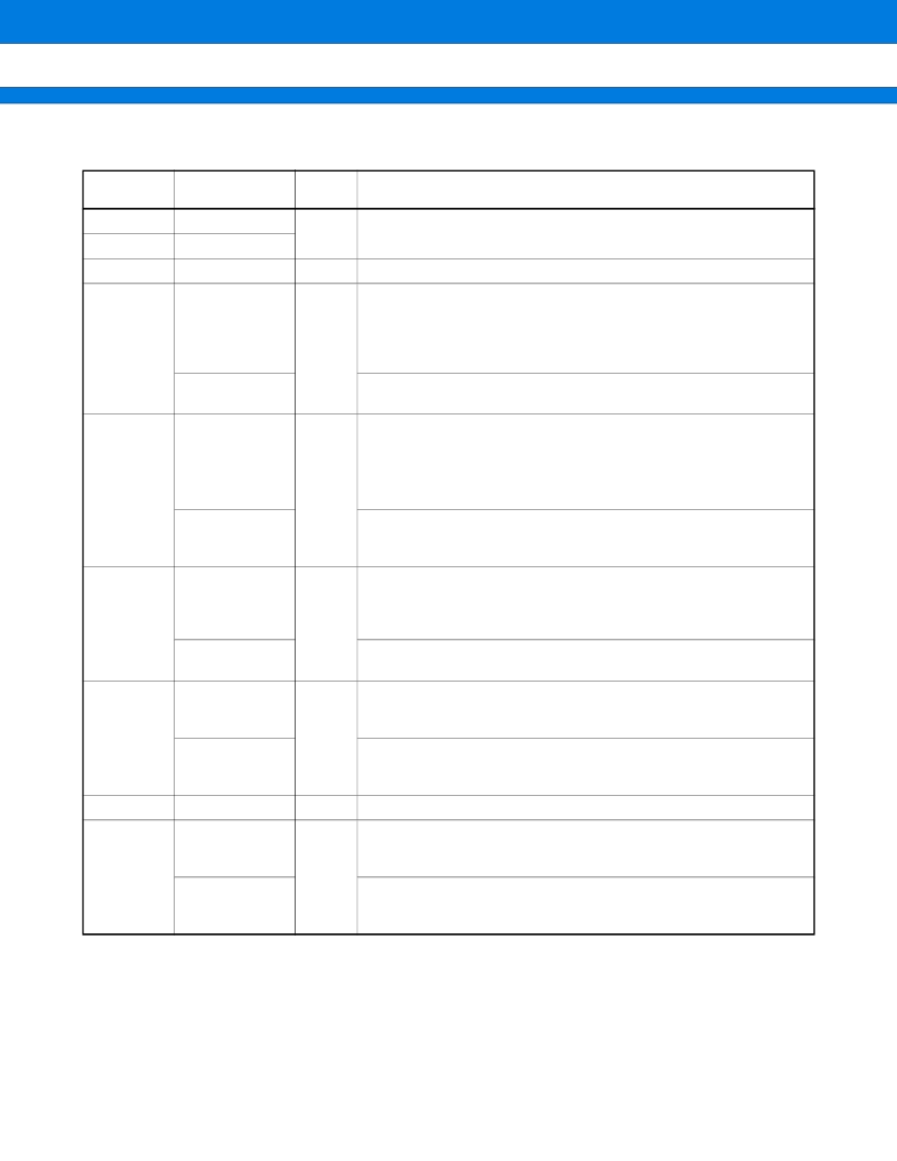
5
MB90230 Series
I
PIN DESCRIPTION
(Continued)
Pin no.
Pin name
Circuit
type
Function
80
X0
A
Oscillator pins
81
X1
82
V
CC
—
Power supply pin
83 to 90
P00 to P07
G
General-purpose I/O port
An input pull-up resistor can be added to the port by setting the
pull-up resistor setting register.
These pins serve as D00 to D07 pins in bus modes other than the
single-chip mode.
D00 to D07
I/O pins for the lower eight bits of the external data bus.
These pins are enabled in an external-bus enabled mode.
91 to 98
P10 to P17
G
General-purpose I/O port
An input pull-up resistor can be added to the port by setting the pull-up
resistor setting register.
These pins are enabled in the single-chip mode with the external-bus
enabled and the 8-bit data bus specified.
D08 to D15
I/O pins for the upper eight bits of the external data bus
These pins are enabled in an external-bus enabled mode with the 16-
bit data bus specified.
99, 100
1 to 6
P20 to P27
G
General-purpose I/O port
An input pull-up resistor can be added to the port by setting the
pull-up resistor setting register.
These pins are enabled in the single-chip mode.
A00 to A07
I/O pins for the lower eight bits of the external data bus
These pins are enabled in an external-bus enabled mode.
7, 8
P30, P31
E
General-purpose I/O port
This port is enabled in the single-chip mode or when the middle
address control register setting is “port.”
A08, A09
I/O pins for the middle eight bits of the external data bus
These pins are enabled in an external-bus enabled mode when the
middle address control register setting is “address.”
9
V
SS
—
Power supply pin
10 to 15
P32 to P37
E
General-purpose I/O port
This port is enabled in the single-chip mode or when the middle
address control register setting is “port.”
A10 to A15
I/O pins for the middle eight bits of the external data bus
These pins are enabled in an external-bus enabled mode when the
middle address control register setting is “address.”
相關PDF資料 |
PDF描述 |
|---|---|
| MB90W234ZFV | 16-bit Proprietary Microcontroller |
| MB90W234 | 16-bit Proprietary Microcontroller |
| MB90V230 | 16-bit Proprietary Microcontroller |
| MB90233 | 16-bit Proprietary Microcontroller |
| MB90233PFV | 16-bit Proprietary Microcontroller |
相關代理商/技術參數(shù) |
參數(shù)描述 |
|---|---|
| MB90V340A-102CR | 制造商:FUJITSU 功能描述: |
| MB-910 | 制造商:Circuit Test 功能描述:BREADBOARD WIRING KIT - 350 PCS |
| MB9100100 | 制造商:COM/DUO 功能描述:FAN 4-6WKS |
| MB9100-100 | 制造商:COM/DUO 功能描述:FAN 4-6WKS |
| MB91101 | 制造商:Panasonic Industrial Company 功能描述:IC |
發(fā)布緊急采購,3分鐘左右您將得到回復。