- 您現(xiàn)在的位置:買賣IC網(wǎng) > PDF目錄377928 > MB90F583BPFV (FUJITSU LTD) 16-bit Proprietary Microcontroller PDF資料下載
參數(shù)資料
| 型號(hào): | MB90F583BPFV |
| 廠商: | FUJITSU LTD |
| 元件分類: | 微控制器/微處理器 |
| 英文描述: | 16-bit Proprietary Microcontroller |
| 中文描述: | 16-BIT, FLASH, 16 MHz, MICROCONTROLLER, PQFP100 |
| 封裝: | PLASTIC, LQFP-100 |
| 文件頁數(shù): | 10/124頁 |
| 文件大小: | 2638K |
| 代理商: | MB90F583BPFV |
第1頁第2頁第3頁第4頁第5頁第6頁第7頁第8頁第9頁當(dāng)前第10頁第11頁第12頁第13頁第14頁第15頁第16頁第17頁第18頁第19頁第20頁第21頁第22頁第23頁第24頁第25頁第26頁第27頁第28頁第29頁第30頁第31頁第32頁第33頁第34頁第35頁第36頁第37頁第38頁第39頁第40頁第41頁第42頁第43頁第44頁第45頁第46頁第47頁第48頁第49頁第50頁第51頁第52頁第53頁第54頁第55頁第56頁第57頁第58頁第59頁第60頁第61頁第62頁第63頁第64頁第65頁第66頁第67頁第68頁第69頁第70頁第71頁第72頁第73頁第74頁第75頁第76頁第77頁第78頁第79頁第80頁第81頁第82頁第83頁第84頁第85頁第86頁第87頁第88頁第89頁第90頁第91頁第92頁第93頁第94頁第95頁第96頁第97頁第98頁第99頁第100頁第101頁第102頁第103頁第104頁第105頁第106頁第107頁第108頁第109頁第110頁第111頁第112頁第113頁第114頁第115頁第116頁第117頁第118頁第119頁第120頁第121頁第122頁第123頁第124頁
MB90580B Series
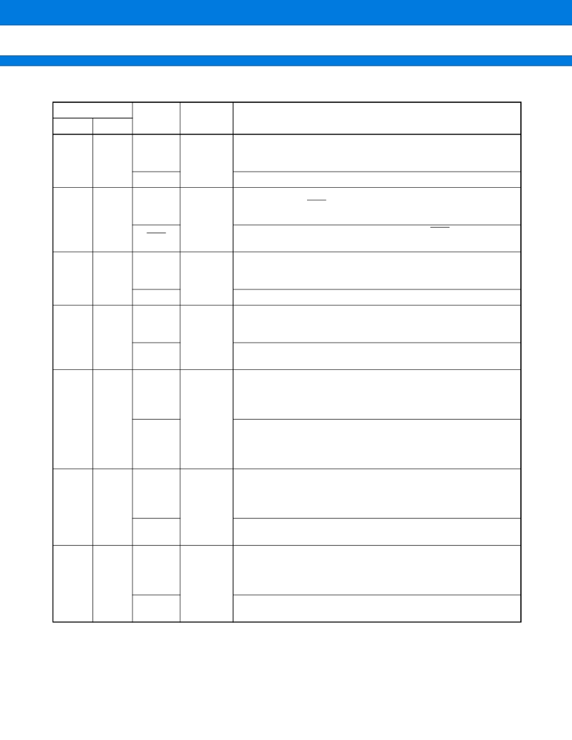
10
*1: FPT-100P-M06
*2: FPT-100P-M05
(Continued)
Pin no.
Pin name
Circuit
type
Function
QFP*
1
LQFP*
2
14
12
P34
F
(CMOS/H)
General-purpose I/O port
Functions as the HRQ pin in external bus mode if the HDE bit in the
EPCR register is “1”.
HRQ
Functions as the hold request input pin (HRQ) in external bus mode.
15
13
P35
F
(CMOS/H)
General-purpose I/O port
Functions as the HAK pin in external bus mode if the HDE bit in the
EPCR register is “1”.
HAK
Functions as the hold acknowledge output pin (HAK) in external bus
mode.
16
14
P36
F
(CMOS/H)
General-purpose I/O port
Functions as the RDY pin in external bus mode if the RYE bit in the
EPCR register is “1”.
RDY
Functions as the external ready input pin (RDY) in external bus mode.
17
15
P37
F
(CMOS/H)
General-purpose I/O port
Functions as the CLK pin in external bus mode if the CKE bit in the
EPCR register is “1”.
CLK
Functions as the machine cycle clock output pin (CLK) in external bus
mode.
18
16
P40
E
(CMOS/H)
General-purpose I/O port.
This pin serves as an open-drain output port with OD40 in the open-
drain control setting register (ODR4) set to “1”. [The pin is disabled
with the input setting (DDR4 register: D40=“0”).]
SIN0
UART0 serial data input (SIN0) pin.
When UART0 is operating for input, this input is used as required and
thus the output from any other function to the pin must be off unless
used intentionally.
19
17
P41
E
(CMOS/H)
General-purpose I/O port.
This pin serves as an open-drain output port with OD41 in the open-
drain control setting register (ODR4) set to “1”. [The pin is disabled
with the input setting (DDR4 register: D41=“0”).]
SOT0
UART0 serial data output pin (SOT0).
This pin is enabled with the UART0 serial data output enabled.
20
18
P42
E
(CMOS/H)
General-purpose I/O port.
This pin serves as an open-drain output port with OD42 in the open-
drain control setting register (ODR4) set to “1”. [The pin is disabled
with the input setting (DDR4 register: D42=“0”).]
SCK0
UART0 serial clock I/O pin (SCK0).
This pin is enabled with the UART0 clock output enabled.
相關(guān)PDF資料 |
PDF描述 |
|---|---|
| MB90583B | 16-bit Proprietary Microcontroller |
| MB90583BPF | 16-bit Proprietary Microcontroller |
| MB90583BPFV | 16-bit Proprietary Microcontroller |
| MB90587PF | Quadruple 2-Input Positive-OR Gate 20-LCCC -55 to 125 |
| MB90587PFV | 16-bit Proprietary Microcontroller |
相關(guān)代理商/技術(shù)參數(shù) |
參數(shù)描述 |
|---|---|
| MB90F583BPMC-GE1 | 制造商:FUJITSU 功能描述: |
| MB90F583CAPFR-GE1 | 制造商:FUJITSU 功能描述: |
| MB90F591GPFR-GE1 | 制造商:FUJITSU 功能描述: |
| MB90F594APFR-GE1 | 制造商:FUJITSU 功能描述: |
| MB90F594GPFR-GE1 | 制造商:FUJITSU 功能描述: |
發(fā)布緊急采購,3分鐘左右您將得到回復(fù)。