- 您現(xiàn)在的位置:買(mǎi)賣(mài)IC網(wǎng) > PDF目錄69018 > MB86605PMT SCSI BUS CONTROLLER, PQFP144 PDF資料下載
參數(shù)資料
| 型號(hào): | MB86605PMT |
| 元件分類: | 總線控制器 |
| 英文描述: | SCSI BUS CONTROLLER, PQFP144 |
| 封裝: | PLASTIC, LQFP-144 |
| 文件頁(yè)數(shù): | 3/64頁(yè) |
| 文件大小: | 275K |
| 代理商: | MB86605PMT |
第1頁(yè)第2頁(yè)當(dāng)前第3頁(yè)第4頁(yè)第5頁(yè)第6頁(yè)第7頁(yè)第8頁(yè)第9頁(yè)第10頁(yè)第11頁(yè)第12頁(yè)第13頁(yè)第14頁(yè)第15頁(yè)第16頁(yè)第17頁(yè)第18頁(yè)第19頁(yè)第20頁(yè)第21頁(yè)第22頁(yè)第23頁(yè)第24頁(yè)第25頁(yè)第26頁(yè)第27頁(yè)第28頁(yè)第29頁(yè)第30頁(yè)第31頁(yè)第32頁(yè)第33頁(yè)第34頁(yè)第35頁(yè)第36頁(yè)第37頁(yè)第38頁(yè)第39頁(yè)第40頁(yè)第41頁(yè)第42頁(yè)第43頁(yè)第44頁(yè)第45頁(yè)第46頁(yè)第47頁(yè)第48頁(yè)第49頁(yè)第50頁(yè)第51頁(yè)第52頁(yè)第53頁(yè)第54頁(yè)第55頁(yè)第56頁(yè)第57頁(yè)第58頁(yè)第59頁(yè)第60頁(yè)第61頁(yè)第62頁(yè)第63頁(yè)第64頁(yè)
11
MB86605
(Continued)
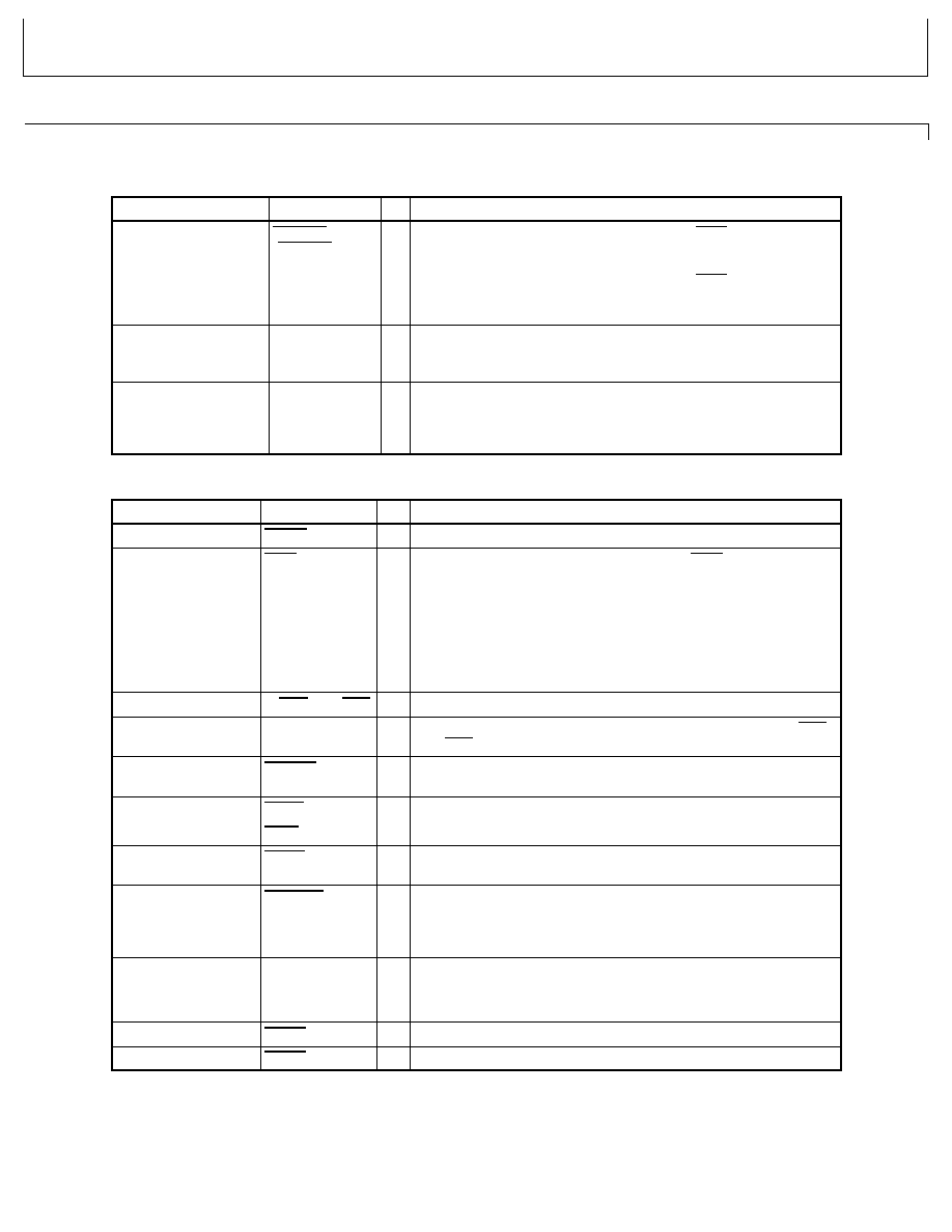
4.
PCI Bus Interface Mode
Pin no.
Pin name
I/O
Function
132
DMBHE
(DMUDS)
I
In 80-series mode: This is used to input the BHE signal output by
the DMAC when the upper byte of the DMA
data bus is valid.
In 68-series mode: This is used to input the UDS signal output by
the DMAC when the upper byte of the DMA
data bus is valid.
125
DMA0
I
This is used to input the address data A0 signal output by the
DMAC in the 80-series mode.
In 68-series mode: Connect to power supply pin (VDD).
126
TP
(Transfer
permission)
I
This is used to input DMA-transfer-enabling signals.
When the TP signal is active, the SPC performs the DMA transfer.
When this signal becomes inactive during DMA transfer, the
transfer stops temporarily at the block boundary.
Pin no.
Pin name
I/O
Function
130
PREQ
O
This pin is used to request the bus arbiter for use of the bus.
129
GNT
I
This is the response signal input pin to the REQ signal from the
bus arbiter.
132, 133, 135, 136,
138, 139, 141, 142,
1, 3 to 5, 7, 9 to 11,
26 to 29, 32 to 34, 36,
38, 39, 41, 42, 44,
46 to 48
AD31 to AD0
I/O PCI 32-bit address and data multiplexed pins
143, 13, 24, 37
C/BE3 to C/BE0
I/O Bus command and Byte Enable signals multiplexed pins.
23
PAR
I/O This is an even parity signal pin for the AD31 to AD0 and C/BE3
to C/BE0 signals. This PAR signal becomes valid after one clock.
14
FRAME
I/O This is a frame signal pin that indicates data are transferring on
the bus.
17
TRDY
I/O Data Ready signal of Target side.
15
IRDY
I/O Data Ready signal of Initiator (Bus master) side.
20
STOP
I/O This is a stop request signal to stop the data transfer from target
to master.
19
DEVSEL
I/O Device select pin. While the device is a target, this pin outputs the
select signal that indicates the self device is selected. While the
device is a master this pin functions as an input pin to indicate
that a device on the bus is selected.
144
IDSEL
I
This is a chip select signal that indicates the configuration access.
126
PCLK
I
PCI bus clock input pin. The maximum clock frequency is 33
MHz.
22
PERR
I/O Data parity error input and output pin.
125
SERR
OD Address parity error output pin.
相關(guān)PDF資料 |
PDF描述 |
|---|---|
| MB86606PMT | SCSI BUS CONTROLLER, PQFP144 |
| MB86612 | 2 CHANNEL(S), 98.304M bps, SERIAL COMM CONTROLLER, PQFP100 |
| MB86703PF | SPECIALTY MICROPROCESSOR CIRCUIT, PQFP80 |
| MB86831-66PFV-G | 32-BIT, 66 MHz, RISC PROCESSOR, PQFP176 |
| MB86832-80PFV-G | 32-BIT, 80 MHz, RISC PROCESSOR, PQFP176 |
相關(guān)代理商/技術(shù)參數(shù) |
參數(shù)描述 |
|---|---|
| MB86606A | 制造商:FUJITSU 制造商全稱:Fujitsu Component Limited. 功能描述:FAST-20 SCSI Protocol Controller |
| MB86606APMT2 | 制造商:FUJITSU 制造商全稱:Fujitsu Component Limited. 功能描述:FAST-20 SCSI Protocol Controller |
| MB86612 | 制造商:FUJITSU 制造商全稱:Fujitsu Component Limited. 功能描述:IEEE 1394 Bus Controller (for MPEG, DVC) |
| MB86612PBT | 制造商:FUJITSU 制造商全稱:Fujitsu Component Limited. 功能描述:IEEE 1394 Bus Controller (for MPEG, DVC) |
| MB86612PFV | 制造商:FUJITSU 制造商全稱:Fujitsu Component Limited. 功能描述:IEEE 1394 Bus Controller (for MPEG, DVC) |
發(fā)布緊急采購(gòu),3分鐘左右您將得到回復(fù)。