- 您現在的位置:買賣IC網 > PDF目錄385552 > MAX847EEI (MAXIM INTEGRATED PRODUCTS INC) 1-Cell, Step-Up Two-Way Pager System IC PDF資料下載
參數資料
| 型號: | MAX847EEI |
| 廠商: | MAXIM INTEGRATED PRODUCTS INC |
| 元件分類: | 電源管理 |
| 英文描述: | 1-Cell, Step-Up Two-Way Pager System IC |
| 中文描述: | 1-CHANNEL POWER SUPPLY MANAGEMENT CKT, PDSO28 |
| 封裝: | 0.150 INCH, 0.025 INCH PITCH, QSOP-28 |
| 文件頁數: | 16/18頁 |
| 文件大小: | 167K |
| 代理商: | MAX847EEI |
M
1-Cell, S tep-Up
Two-Way Pager S ystem IC
16
______________________________________________________________________________________
To minimize battery drain, use large values for R2 and
R4 (>100k
) in the above equations; 470k
is a good
starting value.
See the Low-Noise Analog Supply (REG2) section for
information on selecting R
OFS
.
Since LBO and RSO are open-drain outputs, pull-up
resistors (R5, R6) are usually required. Normally these
will be pulled up to REG1. 100k
is recommended as a
compromise between response time and current drain,
although other values can be used. Since LBI and RSO
are high (open circuit) during normal operation, current
normally does not flow in R5 and R6 until a low-battery
or reset event occurs.
Logic Levels
Note that since the MAX847’s internal logic is powered
from REG1, the input logic levels at the digital inputs:
DR2IN, RUN, SYNC,
CS
, SCL, and SDI, as well as the
logic output levels of SDO, are governed by the voltage
of REG1. Logic high inputs at these pins should not
exceed V
REG1
. Digital inputs should either be driven
from external logic (or a μP) powered from REG1, or by
open-drain logic devices that are pulled up to REG1.
Board Layout and Noise Reduc tion
The MAX847 makes every effort in its internal design to
minimize noise and EMI. Nevertheless, prudent layout
practices are still suggested for best performance.
Recommendations include:
1) Keep trace lengths at L1 and LX1, as well as at
PGND, as short and as wide as possible. Since LX1
swing between V
BAT
and V
OUT
at a high rate, mini-
mizing LX1 trace length serves to reduce the PC
board area that can act as an antenna.
2) The filter capacitors at OUT, REG1, REG2, and
REG3 should be placed as close as possible to
their respective pins (no more than 0.5mm away).
3) A shielded inductor at L1 will minimize radiation
noise, but may not be essential. Toroids will also
exhibit EMI performance similar to that of shielded
coils.
4) The LX1, OUT, and PGND pins are located at the
uppermost part of the IC to facilitate PC layout.
Keep power components in this area to minimize
coupling to other parts of the circuit. Other pins in
this area are digital and are not affected by close
proximity to switching nodes.
5) Use a separate short wide ground trace for PGND
and the ground side of the BATT and OUT filter
capacitors. Tie this trace to the ground plane.
Table 7. External Components
SUPPLIER
INDUCTORS (22μH)
PART NO.
COMMENTS
CD54-220
CD43-220
LQH4N220K
0.94
, 2.6mm high,
low current, low cost
Murata
LQH3C221
0.71
, 2mm high, low
current, low cost
0.18
, 4.5mm high
0.378
, 3.2mm high
0.34
, 3mm high,
shielded
STORAGE CAPACITOR (optional at NICD pin)
Polystor
595D series
A-10300
Tantalum
1.5F
TDK
CAPACITORS
NLC565050-220K
0.43
, 5mm high
Coilcraft
DT1608C-223
0.16
, 3.18mm high,
shielded
AVX
Marcon
Sprague
TPS series
THCR series
595D series
Tantalum
Ceramic
Tantalum
Sumida
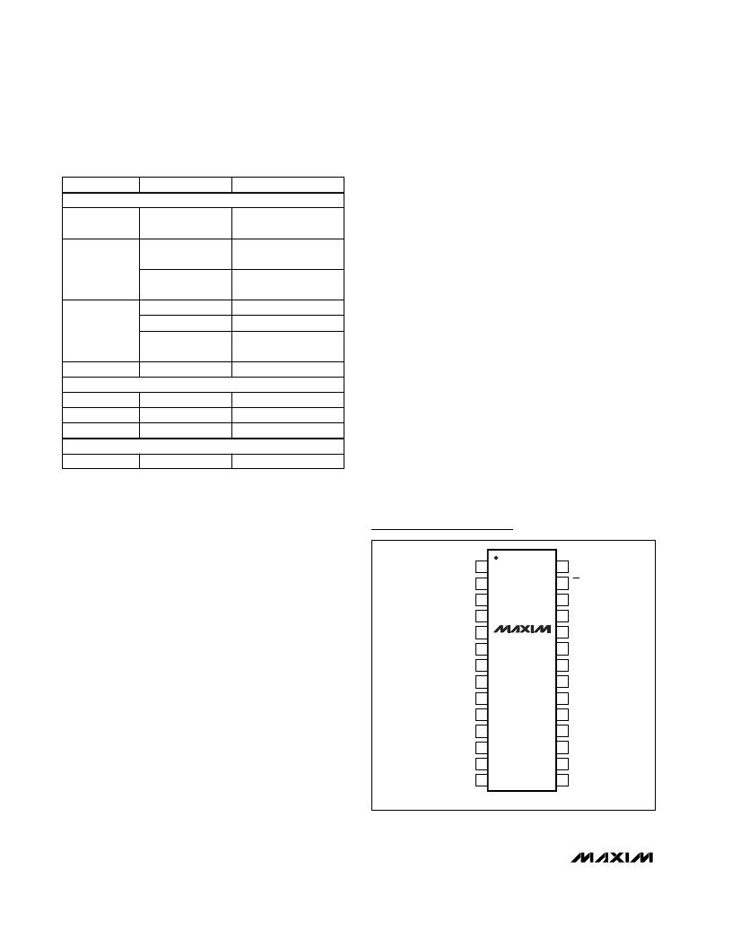
CDRH62B-220
28
27
26
25
24
23
22
21
20
19
18
17
16
15
1
2
3
4
5
6
7
8
9
10
11
12
13
14
RUN
CS
BATT
OUT
REG1
NICD
AGND
R2IN
REG2
REG3
DR2
DR2IN
DR1
DRGND
OFS
SYNC
FILT
LBI
RSIN
CH0
REF
RSO
LBO
SCL
PGND
SDO
SDI
LX1
QSOP
TOP VIEW
MAX847
Pin Configuration
相關PDF資料 |
PDF描述 |
|---|---|
| MAX847 | Quadruple 2-Line To 1-Line Data Selectors/Multiplexers 16-CDIP -55 to 125 |
| MAX848-MAX849 | 1-Cell to 3-Cell, High-Power, Low-Noise, Step-Up DC-DC Converters |
| MAX849ESE | 1-Cell to 3-Cell, High-Power, Low-Noise, Step-Up DC-DC Converters |
| MAX848ESE | 1-Cell to 3-Cell, High-Power, Low-Noise, Step-Up DC-DC Converters |
| MAX848 | Low-Noise, Step-Up DC-DC Converters(高功率,低噪,帶0.5AMOSFET功率開關,步升DC-DC變換器) |
相關代理商/技術參數 |
參數描述 |
|---|---|
| MAX847EEI+ | 功能描述:電池管理 1 Cell Step-Up 2-Way Pager System IC RoHS:否 制造商:Texas Instruments 電池類型:Li-Ion 輸出電壓:5 V 輸出電流:4.5 A 工作電源電壓:3.9 V to 17 V 最大工作溫度:+ 85 C 最小工作溫度:- 40 C 封裝 / 箱體:VQFN-24 封裝:Reel |
| MAX847EEI+T | 功能描述:電池管理 1 Cell Step-Up 2-Way Pager System IC RoHS:否 制造商:Texas Instruments 電池類型:Li-Ion 輸出電壓:5 V 輸出電流:4.5 A 工作電源電壓:3.9 V to 17 V 最大工作溫度:+ 85 C 最小工作溫度:- 40 C 封裝 / 箱體:VQFN-24 封裝:Reel |
| MAX847EEI-C70955 | 制造商:Rochester Electronics LLC 功能描述: 制造商:Maxim Integrated Products 功能描述: |
| MAX847EEI-T | 功能描述:電池管理 1 Cell Step-Up 2-Way Pager System IC RoHS:否 制造商:Texas Instruments 電池類型:Li-Ion 輸出電壓:5 V 輸出電流:4.5 A 工作電源電壓:3.9 V to 17 V 最大工作溫度:+ 85 C 最小工作溫度:- 40 C 封裝 / 箱體:VQFN-24 封裝:Reel |
| MAX847EVKIT | 制造商:Maxim Integrated Products 功能描述:1-CELL STEP-UP TWO-WAY PAGER SYSTE - Rail/Tube |
發(fā)布緊急采購,3分鐘左右您將得到回復。