- 您現(xiàn)在的位置:買賣IC網(wǎng) > PDF目錄17047 > MAX5774EVKIT+ (Maxim Integrated Products)KIT EVAL FOR MAX5774 PDF資料下載
參數(shù)資料
| 型號: | MAX5774EVKIT+ |
| 廠商: | Maxim Integrated Products |
| 文件頁數(shù): | 1/28頁 |
| 文件大?。?/td> | 0K |
| 描述: | KIT EVAL FOR MAX5774 |
| 產(chǎn)品培訓(xùn)模塊: | Lead (SnPb) Finish for COTS Obsolescence Mitigation Program |
| 標準包裝: | 1 |
| DAC 的數(shù)量: | 32 |
| 位數(shù): | 14 |
| 數(shù)據(jù)接口: | 串行 |
| 設(shè)置時間: | 20µs |
| DAC 型: | 電壓 |
| 工作溫度: | 0°C ~ 85°C |
| 已供物品: | 板 |
| 已用 IC / 零件: | MAX5774 |
當(dāng)前第1頁第2頁第3頁第4頁第5頁第6頁第7頁第8頁第9頁第10頁第11頁第12頁第13頁第14頁第15頁第16頁第17頁第18頁第19頁第20頁第21頁第22頁第23頁第24頁第25頁第26頁第27頁第28頁
General Description
The MAX5773/MAX5774/MAX5775 32-channel, 14-bit,
voltage-output, digital-to-analog converters (DACs) are
ideal for applications requiring a high number of pro-
grammable voltages. The MAX5773/MAX5774/
MAX5775 can be programmed to calibrate the 14-bit
input data word for gain and offset errors before updat-
ing the DAC output.
An SPI-/QSPI-/MICROWIRE- or DSP-compatible
serial interface controls the MAX5773/MAX5774/
MAX5775. Each DAC channel has its own input, gain,
and offset register. These three registers pass data
through one of the two multiplier accumulator units
(MACs), resulting in a voltage output corrected for gain
and offset error. Each DAC channel has a double-
buffered input structure to minimize the digital-noise
feedthrough from the digital inputs to the outputs, and
allows for synchronous or asynchronous updating of
the outputs. The DAC outputs update independently or
simultaneously with a single software or hardware com-
mand. The MAX5773/MAX5774/MAX5775 also provide
a digital output (DOUT) that allows for readback or
daisy chaining of multiple devices.
All DAC outputs are buffered and drive 10k
in parallel
with 100pF. The MAX5773 has a 0 to +10V output
range; the MAX5774 has a -2.5V to +7.5V output range;
and the MAX5775 has a -5V to +5V output range.
The MAX5773/MAX5774/MAX5775 are available in a
68-pin, 10mm x 10mm, TQFN package and a 64-pin,
12mm x 12mm, TQFP package. The MAX5773/
MAX5774/MAX5775 are specified over the 0°C to +85°C
temperature range. Refer to the MAX5753/MAX5754/
MAX5755 data sheet for similar 14-bit, 32-channel DACs
without offset and gain calibration.
Applications
Automatic Test Systems
Optical Router Controls
Industrial Process Controls
Arbitrary Function Generators
Avionics Equipment
Minimum Component Count Analog Systems
Digital Offset/Gain Adjustment
Features
o Offset and Gain Correction for Each DAC Channel
o Guaranteed Monotonic to 14 Bits
o 32 Individual DACs in a 10mm x 10mm, 68-Pin
TQFN Package or 12mm x 12mm, 64-Pin TQFP
Package
o Output Voltage Ranges
0 to +10V (MAX5773)
-2.5V to +7.5V (MAX5774)
-5V to +5V (MAX5775)
o Buffered Voltage Outputs Drive 10k || 100pF
o Glitch-Free Power-Up
o SPI/QSPI/MICROWIRE- and DSP-Compatible
33MHz Serial Interface
MAX5773/MAX5774/MAX5775
32-Channel, 14-Bit, Voltage-Output
DACs with Serial Interface
________________________________________________________________
Maxim Integrated Products
1
Ordering Information
19-3686; Rev 2; 4/06
For pricing, delivery, and ordering information, please contact Maxim/Dallas Direct! at
1-888-629-4642, or visit Maxim’s website at www.maxim-ic.com.
EVALUATION
KIT
AVAILABLE
PART
PIN-PACKAGE
OUTPUT
VOLTAGE
RANGE (V)
PKG
CODE
MAX5773UTK*
68 TQFN-EP**
0 to +10
T6800-3
MAX5773UCB*
64 TQFP
0 to +10
C64-12
MAX5774UTK*
68 TQFN-EP**
-2.5 to +7.5
T6800-3
MAX5774UCB
64 TQFP
-2.5 to +7.5
C64-12
MAX5775UTK*
68 TQFN-EP**
-5 to +5
T6800-3
MAX5775UCB*
64 TQFP
-5 to +5
C64-12
Note: All devices are specified over the 0°C to +85°C temper-
ature range.
*
Future product—contact factory for availability.
**
EP = Exposed paddle.
SPI/QSPI are trademarks of Motorola, Inc.
MICROWIRE is a trademark of National Semiconductor Corp.
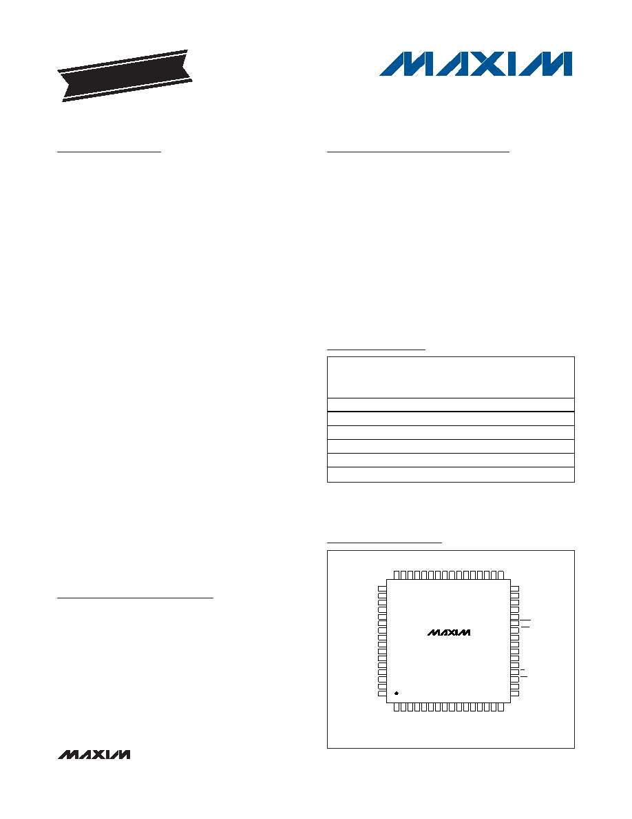
58
59
60
61
62
54
55
56
57
63
38
39
40
41
42
43
44
45
46
47
V
SS
DSP
OUT10
TQFP
TOP VIEW
OUT11
OUT12
OUT13
OUT14
OUT15
AVDD
REFGND
AVCC
OUT31
52
53
49
50
51
OUT30
OUT29
OUT28
OUT27
N.C.
GS2
DOUT
CS
DIN
SCLK
DGND
DVDD
RESET
LDAC
REFGND
GS1
AVDD
REF
VSS
OUT26
OUT25
V
SS
AGND
OUT24
OUT23
OUT22
OUT21
OUT20
OUT19
33
34
35
36
37
OUT18
OUT17
OUT16
N.C.
OUT3
AGND
OUT4
OUT5
OUT6
DV
DD
N.C.
OUT0
OUT1
OUT2
I.C.
OUT7
OUT8
OUT9
48
AV
CC
AV
CC
64
N.C.
DGND
23
22
21
20
19
27
26
25
24
18
29
28
32
31
30
17
11
10
9
8
7
6
5
4
3
2
16
15
14
13
12
1
MAX5773
MAX5774
MAX5775
Pin Configurations
Pin Configurations continued at end of data sheet.
相關(guān)PDF資料 |
PDF描述 |
|---|---|
| MLK1005S3N6S | INDUCTOR MULTILAYER 3.6NH 0402 |
| GBC40DCMD | CONN EDGECARD 80POS .100" WW |
| MLG1005S2N2S | INDUCTOR MULTILAYER 2.2NH 0402 |
| MAX5889EVKIT# | KIT EVALUATION FOR MAX5889 |
| UCS2E181MNY9 | CAP ALUM 180UF 250V 20% RADIAL |
相關(guān)代理商/技術(shù)參數(shù) |
參數(shù)描述 |
|---|---|
| MAX5774EVKIT+ | 功能描述:數(shù)據(jù)轉(zhuǎn)換 IC 開發(fā)工具 MAX5774 Max5774 Eval Kit RoHS:否 制造商:Texas Instruments 產(chǎn)品:Demonstration Kits 類型:ADC 工具用于評估:ADS130E08 接口類型:SPI 工作電源電壓:- 6 V to + 6 V |
| MAX5774UCB+D | 功能描述:數(shù)模轉(zhuǎn)換器- DAC 14-Bit 32Ch Precision DAC RoHS:否 制造商:Texas Instruments 轉(zhuǎn)換器數(shù)量:1 DAC 輸出端數(shù)量:1 轉(zhuǎn)換速率:2 MSPs 分辨率:16 bit 接口類型:QSPI, SPI, Serial (3-Wire, Microwire) 穩(wěn)定時間:1 us 最大工作溫度:+ 85 C 安裝風(fēng)格:SMD/SMT 封裝 / 箱體:SOIC-14 封裝:Tube |
| MAX5774UCB+TD | 功能描述:數(shù)模轉(zhuǎn)換器- DAC 14-Bit 32Ch Precision DAC RoHS:否 制造商:Texas Instruments 轉(zhuǎn)換器數(shù)量:1 DAC 輸出端數(shù)量:1 轉(zhuǎn)換速率:2 MSPs 分辨率:16 bit 接口類型:QSPI, SPI, Serial (3-Wire, Microwire) 穩(wěn)定時間:1 us 最大工作溫度:+ 85 C 安裝風(fēng)格:SMD/SMT 封裝 / 箱體:SOIC-14 封裝:Tube |
| MAX5774UCB-D | 功能描述:數(shù)模轉(zhuǎn)換器- DAC RoHS:否 制造商:Texas Instruments 轉(zhuǎn)換器數(shù)量:1 DAC 輸出端數(shù)量:1 轉(zhuǎn)換速率:2 MSPs 分辨率:16 bit 接口類型:QSPI, SPI, Serial (3-Wire, Microwire) 穩(wěn)定時間:1 us 最大工作溫度:+ 85 C 安裝風(fēng)格:SMD/SMT 封裝 / 箱體:SOIC-14 封裝:Tube |
| MAX5774UCB-TD | 功能描述:數(shù)模轉(zhuǎn)換器- DAC RoHS:否 制造商:Texas Instruments 轉(zhuǎn)換器數(shù)量:1 DAC 輸出端數(shù)量:1 轉(zhuǎn)換速率:2 MSPs 分辨率:16 bit 接口類型:QSPI, SPI, Serial (3-Wire, Microwire) 穩(wěn)定時間:1 us 最大工作溫度:+ 85 C 安裝風(fēng)格:SMD/SMT 封裝 / 箱體:SOIC-14 封裝:Tube |
發(fā)布緊急采購,3分鐘左右您將得到回復(fù)。