- 您現(xiàn)在的位置:買賣IC網(wǎng) > PDF目錄11565 > MAX3420EETG+T (Maxim Integrated Products)IC USB PERIPH CONTROLLER 24TQFN PDF資料下載
參數(shù)資料
| 型號: | MAX3420EETG+T |
| 廠商: | Maxim Integrated Products |
| 文件頁數(shù): | 4/22頁 |
| 文件大小: | 0K |
| 描述: | IC USB PERIPH CONTROLLER 24TQFN |
| 產(chǎn)品培訓(xùn)模塊: | Lead (SnPb) Finish for COTS Obsolescence Mitigation Program |
| 標(biāo)準(zhǔn)包裝: | 2,500 |
| 控制器類型: | USB 外設(shè)控制器 |
| 接口: | USB/串行 |
| 電源電壓: | 3 V ~ 3.6 V |
| 電流 - 電源: | 15mA |
| 工作溫度: | -40°C ~ 85°C |
| 安裝類型: | 表面貼裝 |
| 封裝/外殼: | 24-WFQFN 裸露焊盤 |
| 供應(yīng)商設(shè)備封裝: | 24-TQFN-EP(4x4) |
| 包裝: | 帶卷 (TR) |
| 配用: | MAX3420EEVKIT-2+-ND - EVAL KIT FOR MAX3420E |
USB Peripheral Controller
with SPI Interface
Typical Operating Characteristics
(VCC = +3.3V, VL = +3.3V, TA = +25°C.)
Detailed Description
The MAX3420E contains the digital logic and analog
circuitry necessary to implement a full-speed USB
peripheral that complies with the USB specification rev
2.0. ESD protection of ±15kV is provided on D+, D-,
and VBCOMP. The MAX3420E features an internal USB
transceiver and an internal 1.5k
Ω resistor that connects
between D+ and VCC under the control of a register bit
(CONNECT). This allows a USB peripheral to control
the logical connection to the USB host. Any SPI master
can communicate with the MAX3420E through the SPI
slave interface that operates in SPI mode (0,0) or (1,1).
An SPI master accesses the MAX3420E by reading and
writing to internal registers. A typical data transfer con-
sists of writing a first byte that sets a register address
and direction with additional bytes reading or writing
data to the register or internal FIFO.
The MAX3420E contains 384 bytes of endpoint buffer
memory, implementing the following endpoints:
EP0: 64-byte bidirectional CONTROL endpoint
EP1: 2 x 64-byte double-buffered BULK/INT
OUT endpoint
EP2: 2 x 64-byte double-buffered BULK/INT IN
endpoint
EP3: 64-byte BULK/INT IN endpoint
The choice to use EP1, EP2, EP3 as BULK or INTER-
RUPT endpoints is strictly a function of the endpoint
descriptors that the SPI master returns to the USB host
during enumeration.
The MAX3420E register set and SPI interface is optimized
to reduce SPI traffic. An interrupt output pin, INT, notifies
the SPI master when USB service is required: when a
packet arrives, a packet is sent, or the host suspends or
resumes bus activity. Double-buffered endpoints help
sustain bandwidth by allowing data to move concurrently
over USB and the SPI interface.
VCC
Power the USB transceiver by applying a positive 3.3V
supply to VCC. Bypass VCC to GND with a 1.0F
ceramic capacitor as close to the VCC pin as possible.
VL
The MAX3420E digital core is powered though the VL
pin. VL also acts as a reference level for the SPI inter-
face and all other inputs and outputs. Connect VL to the
system’s logic-level power supply. Internal level transla-
tors and VL allow the SPI interface and all general-pur-
pose inputs and outputs to operate at a system voltage
between 1.71V and 3.6V.
VBCOMP
The MAX3420E features a USB VBUS detector input,
VBCOMP. The VBCOMP pin can withstand input volt-
ages up to 6V. Bypass VBCOMP to GND with a 1.0F
ceramic capacitor. According to USB specification rev
2.0, a self-powered USB device must not power the
1.5k
Ω pullup resistor on D+ if the USB host turns off
VBUS. VBCOMP is internally connected to a voltage
comparator so that the SPI master can detect the loss
of VBUS (through an interrupt (INT) or checking a bit
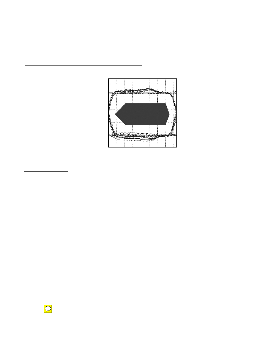
EYE DIAGRAM
MAX3420E
toc01
4
1
0
-1
0
1020304050607080
2
3
TIME (ns)
D+
AND
D-
(V)
MAX3420E
12
Maxim Integrated
相關(guān)PDF資料 |
PDF描述 |
|---|---|
| V375C28M75B | CONVERTER MOD DC/DC 28V 75W |
| MAX5942BESE+T | IC IEEE 802.3AF POE SYSTM 16SOIC |
| MAX5942AESE+T | IC IEEE 802.3AF POE SYSTM 16SOIC |
| PIC18LF23K22-E/SS | IC MCU 8BIT 8KB FLASH 28SSOP |
| V375A24C400BF2 | CONVERTER MOD DC/DC 24V 400W |
相關(guān)代理商/技術(shù)參數(shù) |
參數(shù)描述 |
|---|---|
| MAX3420EEVKIT | 制造商:Maxim Integrated Products 功能描述:MAX3420E EVAL KIT - Bulk |
| MAX3420EEVKIT-2+ | 功能描述:界面開發(fā)工具 MAX3420E Eval Kit RoHS:否 制造商:Bourns 產(chǎn)品:Evaluation Boards 類型:RS-485 工具用于評估:ADM3485E 接口類型:RS-485 工作電源電壓:3.3 V |
| MAX3421E | 制造商:Maxim Integrated Products 功能描述:USB PERIPHERAL/HOST CONTROLLER WITH SPI INTERFACE - Rail/Tube |
| MAX3421EEHJ+ | 功能描述:外圍驅(qū)動器與原件 - PCI USB Peripheral Controller w/SPI RoHS:否 制造商:PLX Technology 工作電源電壓: 最大工作溫度: 安裝風(fēng)格:SMD/SMT 封裝 / 箱體:FCBGA-1156 封裝:Tray |
| MAX3421EEHJ+T | 功能描述:外圍驅(qū)動器與原件 - PCI USB Peripheral Controller w/SPI RoHS:否 制造商:PLX Technology 工作電源電壓: 最大工作溫度: 安裝風(fēng)格:SMD/SMT 封裝 / 箱體:FCBGA-1156 封裝:Tray |
發(fā)布緊急采購,3分鐘左右您將得到回復(fù)。