- 您現(xiàn)在的位置:買(mǎi)賣(mài)IC網(wǎng) > PDF目錄384656 > MAX2463EAI (MAXIM INTEGRATED PRODUCTS INC) 900MHz Image-Reject Transceivers PDF資料下載
參數(shù)資料
| 型號(hào): | MAX2463EAI |
| 廠商: | MAXIM INTEGRATED PRODUCTS INC |
| 元件分類(lèi): | 無(wú)繩電話/電話 |
| 英文描述: | 900MHz Image-Reject Transceivers |
| 中文描述: | TELECOM, CELLULAR, RF AND BASEBAND CIRCUIT, PDSO28 |
| 封裝: | 5.30 MM, MO-150, SSOP-28 |
| 文件頁(yè)數(shù): | 8/14頁(yè) |
| 文件大?。?/td> | 250K |
| 代理商: | MAX2463EAI |
第1頁(yè)第2頁(yè)第3頁(yè)第4頁(yè)第5頁(yè)第6頁(yè)第7頁(yè)當(dāng)前第8頁(yè)第9頁(yè)第10頁(yè)第11頁(yè)第12頁(yè)第13頁(yè)第14頁(yè)
M
900MHz Image-Reject Transceivers
8
_______________________________________________________________________________________
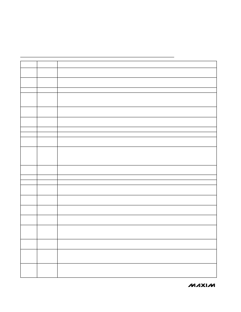
Pin Description
Supply Voltage Input for Receive Low-Noise Amplifier. Bypass with a 47pF low-inductance capacitor to
GND (pin 7 if possible).
Ground Connection for Receive Low-Noise Amplifier
Ground Connection for Signal-Path Blocks, except LNA
6
Receiver RF Input, single-ended. The input match shown in Figure 1 maintains an input VSWR of better
than 2:1 from 902MHz to 928MHz.
5
Transmit Gain-Control Input. Connect to V
CC
for highest gain and best temperature stability. When
driven with a control voltage, the IF buffer gain can be adjusted over a 36dB range (see
Typical
Operating Characteristics
).
4
V
CC
RXIN
TXGAIN
Prescaler/Oscillator Buffer Output. In divide-by-64/65 mode (DIV1 = low), the output level is 500mVp-p
into a high-impedance load. In divide-by-1 mode (DIV1 = high), this output delivers -8dBm into a 50
load. AC couple to this pin.
21
Transmit Bias Compensation Pin. Bypass with a 47pF low-inductance capacitor and 0.01μF to GND.
Do not make any other connections to this pin.
14
No Connect. Not internally connected.
13
Ground connection for the Prescaler. Tie PREGND to ground for normal operation. Leave floating to
disable the prescaler and the output buffer. Tie MOD and DIV1 to ground and leave PREOUT floating
when disabling the prescaler.
CAP2
N.C.
Transmitter IF Input, 330
, single-ended. AC couple to this pin.
12
Single-Ended, 330
IF Output. AC couple to this pin.
3
Receive Bias Compensation Pin. Bypass with a 47pF low-inductance capacitor and 0.01μF to GND.
Do not make any other connections to this pin.
2
Supply-Voltage Input for Master Bias Cell. Bypass with a 47pF low-inductance capacitor and 0.1μF to
GND (pin 28, if possible).
1
FUNCTION
PIN
Low-Noise Amplifier Gain-Control Input. Drive this pin high for maximum gain. When LNAGAIN is pulled
low, the LNA is capacitively bypassed and the supply current is reduced by 4.5mA. This pin can also be
driven with an analog voltage to adjust the LNA gain in intermediate states. Refer to the Receiver Gain
vs. LNAGAIN Voltage graph in the
Typical Operating Characteristics,
as well as Table 1.
10
PA Predriver Output. See Figure 1 for an example matching network, which provides better than 2:1
VSWR from 902MHz to 928MHz.
9
TXIN
LNAGAIN
TXOUT
7
8
GND
GND
RXOUT
CAP1
V
CC
NAME
Supply Voltage Input for Signal-Path Blocks, except LNA. Bypass with a 47pF low-inductance capacitor
and 0.01μF to GND (pin 8, if possible).
11
V
CC
20
PREOUT
PREGND
Modulus Control for the Divide-by-64/65 Prescaler: high = divide-by-64, low = divide-by-65. Note that
the DIV1 pin must be at logic low when using the prescaler mode.
19
Driving VCOON with a logic high turns on the VCO, phase shifters, VCO buffers, and prescaler. The
prescaler can be selectively disabled by floating the PREGND pin.
17
Driving RXON with a logic high enables the LNA, receive mixer, and IF output buffer. VCOON must also
be high.
16
MOD
VCOON
RXON
Driving TXON with a logic high enables the transmit IF variable-gain amplifier, upconverter mixer, and PA
predriver. VCOON must also be high.
15
TXON
Driving DIV1 with a logic high disables the divide-by-64/65 prescaler and connects the PREOUT pin
directly to an oscillator buffer amplifier, which outputs -8dBm into a 50
load. Tie DIV1 low for divide-by-
64/65 operation. Pull this pin low when in shutdown to minimize off current.
18
DIV1
相關(guān)PDF資料 |
PDF描述 |
|---|---|
| MAX2421EAI | 900MHz Image-Reject Transceivers |
| MAX2460EAI | 900MHz Image-Reject Transceivers |
| MAX2420 | Hex Buffers/Drivers With Open-Collector High-Voltage Outputs 14-SO 0 to 70 |
| MAX2422EAI | Hex Buffers/Drivers With Open-Collector High-Voltage Outputs 14-SO 0 to 70 |
| MAX2420EAI | 900MHz Image-Reject Transceivers |
相關(guān)代理商/技術(shù)參數(shù) |
參數(shù)描述 |
|---|---|
| MAX2463EAI+ | 功能描述:射頻收發(fā)器 Integrated Circuits (ICs) RoHS:否 制造商:Atmel 頻率范圍:2322 MHz to 2527 MHz 最大數(shù)據(jù)速率:2000 Kbps 調(diào)制格式:OQPSK 輸出功率:4 dBm 類(lèi)型: 工作電源電壓:1.8 V to 3.6 V 最大工作溫度:+ 85 C 接口類(lèi)型:SPI 封裝 / 箱體:QFN-32 封裝:Tray |
| MAX2463EAI+T | 功能描述:射頻收發(fā)器 Integrated Circuits (ICs) RoHS:否 制造商:Atmel 頻率范圍:2322 MHz to 2527 MHz 最大數(shù)據(jù)速率:2000 Kbps 調(diào)制格式:OQPSK 輸出功率:4 dBm 類(lèi)型: 工作電源電壓:1.8 V to 3.6 V 最大工作溫度:+ 85 C 接口類(lèi)型:SPI 封裝 / 箱體:QFN-32 封裝:Tray |
| MAX2463EAI-T | 功能描述:射頻收發(fā)器 RoHS:否 制造商:Atmel 頻率范圍:2322 MHz to 2527 MHz 最大數(shù)據(jù)速率:2000 Kbps 調(diào)制格式:OQPSK 輸出功率:4 dBm 類(lèi)型: 工作電源電壓:1.8 V to 3.6 V 最大工作溫度:+ 85 C 接口類(lèi)型:SPI 封裝 / 箱體:QFN-32 封裝:Tray |
| MAX2463EVKIT-SO | 功能描述:射頻開(kāi)發(fā)工具 RoHS:否 制造商:Taiyo Yuden 產(chǎn)品:Wireless Modules 類(lèi)型:Wireless Audio 工具用于評(píng)估:WYSAAVDX7 頻率: 工作電源電壓:3.4 V to 5.5 V |
| MAX246CPL | 功能描述:RS-232接口集成電路 RoHS:否 制造商:Exar 數(shù)據(jù)速率:52 Mbps 工作電源電壓:5 V 電源電流:300 mA 工作溫度范圍:- 40 C to + 85 C 安裝風(fēng)格:SMD/SMT 封裝 / 箱體:LQFP-100 封裝: |
發(fā)布緊急采購(gòu),3分鐘左右您將得到回復(fù)。