- 您現(xiàn)在的位置:買賣IC網(wǎng) > PDF目錄383313 > MAX1205CMH (MAXIM INTEGRATED PRODUCTS INC) +5v sINGLE-sUPPLY, 1mSPS, 14-bIT sELF-cALIBRATING adc PDF資料下載
參數(shù)資料
| 型號(hào): | MAX1205CMH |
| 廠商: | MAXIM INTEGRATED PRODUCTS INC |
| 元件分類: | ADC |
| 英文描述: | +5v sINGLE-sUPPLY, 1mSPS, 14-bIT sELF-cALIBRATING adc |
| 中文描述: | 1-CH 14-BIT PROPRIETARY METHOD ADC, PARALLEL ACCESS, PQFP44 |
| 封裝: | M0-108AA-2, MQFP-44 |
| 文件頁(yè)數(shù): | 9/12頁(yè) |
| 文件大?。?/td> | 127K |
| 代理商: | MAX1205CMH |
external amplifiers to compensate for any resistive drop
on these lines, internal or external to the chip. Ensure a
correct reference voltage by using proper Kelvin con-
nections at the sense pins.
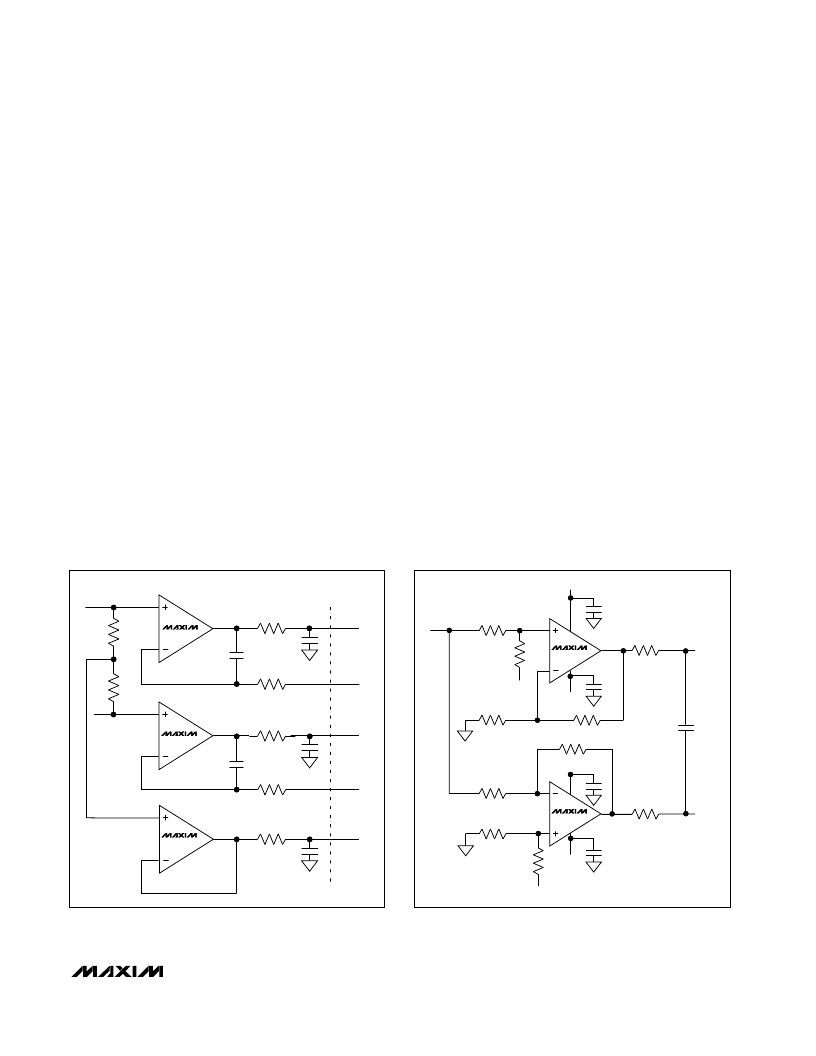
Common-Mode V oltage
The switched capacitor input circuit at the analog input
allows signals between AGND and the analog power
supply. Since the common-mode voltage has a strong
influence on the performance of the ADC, the best
results are obtained by choosing V
CM
to be at half the
difference between the reference voltages V
RFP
and
V
RFN
. Achieve this by using a resistive divider between
the two reference potentials. Figure 4 shows a typical
driving circuit for good dynamic performance.
Analog S ignal Conditioning
For single-ended inputs the negative analog input pin
(INN) is connected to the common-mode voltage pin
(CM), and the positive analog input pin (INP) is con-
nected to the input.
To take full advantage of the ADC’s superior AC perfor-
mance up to the Nyquist frequency, drive the chip with
differential signals. In communication systems, the sig-
nals may inherently be available in differential mode.
Medical and/or other applications may only provide sin-
gle-ended inputs. In this case, convert the single-
ended signals into differential ones by using the circuit
recommended in Figure 5. Use low-noise, wideband
amplifiers such as the MAX4108 to maintain the signal
purity over the full-power bandwidth of the MAX1205
input.
Lowpass or bandpass signals may be required to
improve the signal-to-noise-and-distortion ratio of the
incoming signal. For low-frequency signals (<100kHz),
active filters may be used. For higher frequencies, pas-
sive filters are more convenient.
S ingle-Ended to Differential
Conversion Using T ransformers
An alternative single-ended to differential-ended con-
version method is a balun transformer such as the
CTX03-13675 from Coiltronics. An important benefit of
these transformers is their ability to level-shift single-
ended signals referred to ground on the primary side to
optimum common-mode voltages on the secondary
side. At frequencies below 20kHz, the transformer core
begins to saturate, causing odd-order harmonics.
Cloc k S ourc e Requirements
Pipelined ADCs typically need a 50% duty cycle clock.
To avoid this constraint, the MAX1205 provides a
M
+5V S ingle-S upply, 1Msps, 14-Bit
S elf-Calibrating ADC
_______________________________________________________________________________________
9
RFP = 4.096V
RFN = 0V
5k
5k
MAX410
CHIP BOUNDARY
CM
RFNS
RFNF
RFPS
RFPF
MAX410
MAX410
Figure 4. Drive Circuit for the Reference Pins and the Common-
Mode Pin
MAX4108
INP
INN
CM
V-
V+
IN
CM
V+
V-
MAX4108
Figure 5. A simple circuit generates differential signals from a
single-ended input referred to analog ground. The common-
mode voltage at INP and INN is the same as CM.
相關(guān)PDF資料 |
PDF描述 |
|---|---|
| MAX121EAP | 308Ksps ADC with DSP Interface and 78dB SINAD |
| MAX121EWE | 308Ksps ADC with DSP Interface and 78dB SINAD |
| MAX121CAP | 308Ksps ADC with DSP Interface and 78dB SINAD |
| MAX121EVKIT-DIP | 308Ksps ADC with DSP Interface and 78dB SINAD |
| MAX121MJE | 308Ksps ADC with DSP Interface and 78dB SINAD |
相關(guān)代理商/技術(shù)參數(shù) |
參數(shù)描述 |
|---|---|
| MAX1205CMH+ | 制造商:Maxim Integrated Products 功能描述:ADC SGL PIPELINED 1MSPS 14BIT PARALLEL 44MQFP - Rail/Tube |
| MAX1205CMH+T | 制造商:Maxim Integrated Products 功能描述:ADC SGL PIPELINED 1MSPS 14BIT PARALLEL 44MQFP - Tape and Reel |
| MAX1205CMH-T | 制造商:Maxim Integrated Products 功能描述:44 PINS MQFP PKG - Tape and Reel |
| MAX1205EMH | 制造商:Maxim Integrated Products 功能描述:44 PINS MQFP PKG - Bulk |
| MAX1205EMH+ | 制造商:Maxim Integrated Products 功能描述:ADC SGL PIPELINED 1MSPS 14BIT PARALLEL 44MQFP - Rail/Tube |
發(fā)布緊急采購(gòu),3分鐘左右您將得到回復(fù)。