- 您現(xiàn)在的位置:買賣IC網(wǎng) > PDF目錄383312 > MAX1185ECM (MAXIM INTEGRATED PRODUCTS INC) Dual 10-Bit, 20Msps, +3V, Low-Power ADC with Internal Reference and Multiplexed Parallel Outputs PDF資料下載
參數(shù)資料
| 型號: | MAX1185ECM |
| 廠商: | MAXIM INTEGRATED PRODUCTS INC |
| 元件分類: | ADC |
| 英文描述: | Dual 10-Bit, 20Msps, +3V, Low-Power ADC with Internal Reference and Multiplexed Parallel Outputs |
| 中文描述: | 2-CH 10-BIT FLASH METHOD ADC, PARALLEL ACCESS, PQFP48 |
| 封裝: | 7 X 7 MM, TQFP-48 |
| 文件頁數(shù): | 14/20頁 |
| 文件大小: | 495K |
| 代理商: | MAX1185ECM |
M
Dual 10-Bit, 20Msps, +3V, Low-Power ADC with
Internal Reference and Multiplexed Parallel Outputs
14
______________________________________________________________________________________
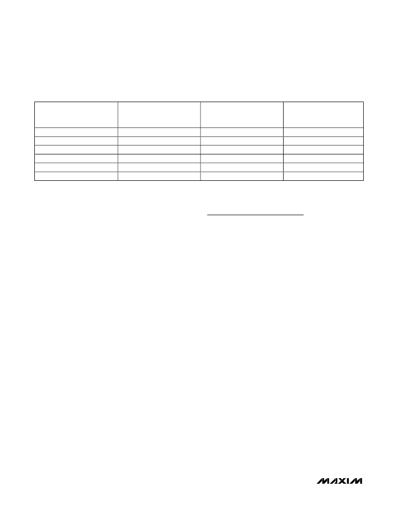
Table 1. MAX1185 Output Codes For Differential Inputs
*
V
REF
= V
REFP
- V
REFN
DIFFERENTIAL INPUT
VOLTAGE*
DIFFERENTIAL
INPUT
STRAIGHT OFFSET
BINARY
T/B = 0
TWO
’
S COMPLEMENT
T/B = 1
V
REF
x 511/512
V
REF
x 1/512
0
- V
REF
x 1/512
-V
REF
x 511/512
-V
REF
x 512/512
+FULL SCALE - 1LSB
+ 1 LSB
Bipolar Zero
- 1 LSB
- FULL SCALE + 1 LSB
- FULL SCALE
11 1111 1111
10 0000 0001
10 0000 0000
01 1111 1111
00 0000 0001
00 0000 0000
01 1111 1111
00 0000 0001
00 0000 0000
11 1111 1111
10 0000 0001
10 0000 0000
Single-Ended AC-Coupled Input Signal
Figure 7 shows an AC-coupled, single-ended applica-
tion. Amplifiers like the MAX4108 provide high speed,
high bandwidth, low noise, and low distortion to maintain
the integrity of the input signal.
Typical QAM Demodulation Application
The most frequently used modulation technique for digital
communications applications is probably the Quadrature
Amplitude Modulation (QAM). Typically found in spread-
spectrum based systems, a QAM signal represents a
carrier frequency modulated in both amplitude and
phase. At the transmitter, modulating the baseband sig-
nal with quadrature outputs, a local oscillator followed by
subsequent up-conversion can generate the QAM signal.
The result is an in-phase (I) and a quadrature (Q) carrier
component, where the Q component is 90 degree phase-
shifted with respect to the in-phase component. At the
receiver, the QAM signal is divided down into it
’
s I and Q
components, essentially representing the modulation
process reversed. Figure 8 displays the demodulation
process performed in the analog domain, using the dual
matched +3.3V, 10-bit ADC MAX1185 and the MAX2451
quadrature demodulator to recover and digitize the I and
Q baseband signals. Before being digitized by the
MAX1185, the mixed down-signal components may be fil-
tered by matched analog filters, such as Nyquist or
Pulse-Shaping filters. These remove any unwanted
images from the mixing process, thereby enhancing the
overall signal-to-noise (SNR) performance and minimizing
intersymbol interference.
Grounding, Bypassing, and
Board Layout
The MAX1185 requires high-speed board layout design
techniques. Locate all bypass capacitors as close to
the device as possible, preferably on the same side as
the ADC, using surface-mount devices for minimum
inductance. Bypass V
DD
, REFP, REFN, and COM with
two parallel 0.1μF ceramic capacitors and a 2.2μF
bipolar capacitor to GND. Follow the same rules to
bypass the digital supply (OV
DD
) to OGND. Multilayer
boards with separated ground and power planes pro-
duce the highest level of signal integrity. Consider the
use of a split ground plane arranged to match the
physical location of the analog ground (GND) and the
digital output driver ground (OGND) on the ADC
’
s
package. The two ground planes should be joined at a
single point such that the noisy digital ground currents
do not interfere with the analog ground plane. The ideal
location of this connection can be determined experi-
mentally at a point along the gap between the two
ground planes, which produces optimum results. Make
this connection with a low-value, surface-mount resistor
(1
to 5
), a ferrite bead, or a direct short. Alternatively,
all ground pins could share the same ground plane, if
the ground plane is sufficiently isolated from any noisy
digital systems ground plane (e.g., downstream output
buffer or DSP ground plane). Route high-speed digital
signal traces away from the sensitive analog traces of
either channel. Make sure to isolate the analog input
lines to each respective converter to minimize channel-
to-channel crosstalk. Keep all signal lines short and
free of 90 degree turns.
相關(guān)PDF資料 |
PDF描述 |
|---|---|
| MAX1190 | Dual 10-Bit, 120Msps, 3.3V, Low-Power ADC with Internal Reference and Parallel Outputs |
| MAX1190ECM | Dual 10-Bit, 120Msps, 3.3V, Low-Power ADC with Internal Reference and Parallel Outputs |
| MAX1191 | Ultra-Low-Power, 7.5Msps, Dual 8-Bit ADC |
| MAX1191ETI-T | Ultra-Low-Power, 7.5Msps, Dual 8-Bit ADC |
| MAX1198 | Dual, 8-Bit, 100Msps, 3.3V, Low-Power ADC with Internal Reference and Parallel Outputs |
相關(guān)代理商/技術(shù)參數(shù) |
參數(shù)描述 |
|---|---|
| MAX1185ECM/V+ | 功能描述:模數(shù)轉(zhuǎn)換器 - ADC 10-Bit 2Ch 20Msps High Speed ADC RoHS:否 制造商:Texas Instruments 通道數(shù)量:2 結(jié)構(gòu):Sigma-Delta 轉(zhuǎn)換速率:125 SPs to 8 KSPs 分辨率:24 bit 輸入類型:Differential 信噪比:107 dB 接口類型:SPI 工作電源電壓:1.7 V to 3.6 V, 2.7 V to 5.25 V 最大工作溫度:+ 85 C 安裝風(fēng)格:SMD/SMT 封裝 / 箱體:VQFN-32 |
| MAX1185ECM/V+T | 功能描述:模數(shù)轉(zhuǎn)換器 - ADC 10-Bit 2Ch 20Msps High Speed ADC RoHS:否 制造商:Texas Instruments 通道數(shù)量:2 結(jié)構(gòu):Sigma-Delta 轉(zhuǎn)換速率:125 SPs to 8 KSPs 分辨率:24 bit 輸入類型:Differential 信噪比:107 dB 接口類型:SPI 工作電源電壓:1.7 V to 3.6 V, 2.7 V to 5.25 V 最大工作溫度:+ 85 C 安裝風(fēng)格:SMD/SMT 封裝 / 箱體:VQFN-32 |
| MAX1185ECM+D | 功能描述:模數(shù)轉(zhuǎn)換器 - ADC 10-Bit 2Ch 20Msps High Speed ADC RoHS:否 制造商:Texas Instruments 通道數(shù)量:2 結(jié)構(gòu):Sigma-Delta 轉(zhuǎn)換速率:125 SPs to 8 KSPs 分辨率:24 bit 輸入類型:Differential 信噪比:107 dB 接口類型:SPI 工作電源電壓:1.7 V to 3.6 V, 2.7 V to 5.25 V 最大工作溫度:+ 85 C 安裝風(fēng)格:SMD/SMT 封裝 / 箱體:VQFN-32 |
| MAX1185ECM+TD | 功能描述:模數(shù)轉(zhuǎn)換器 - ADC 10-Bit 2Ch 20Msps High Speed ADC RoHS:否 制造商:Texas Instruments 通道數(shù)量:2 結(jié)構(gòu):Sigma-Delta 轉(zhuǎn)換速率:125 SPs to 8 KSPs 分辨率:24 bit 輸入類型:Differential 信噪比:107 dB 接口類型:SPI 工作電源電壓:1.7 V to 3.6 V, 2.7 V to 5.25 V 最大工作溫度:+ 85 C 安裝風(fēng)格:SMD/SMT 封裝 / 箱體:VQFN-32 |
| MAX1185ECM-D | 功能描述:模數(shù)轉(zhuǎn)換器 - ADC RoHS:否 制造商:Texas Instruments 通道數(shù)量:2 結(jié)構(gòu):Sigma-Delta 轉(zhuǎn)換速率:125 SPs to 8 KSPs 分辨率:24 bit 輸入類型:Differential 信噪比:107 dB 接口類型:SPI 工作電源電壓:1.7 V to 3.6 V, 2.7 V to 5.25 V 最大工作溫度:+ 85 C 安裝風(fēng)格:SMD/SMT 封裝 / 箱體:VQFN-32 |
發(fā)布緊急采購,3分鐘左右您將得到回復(fù)。