- 您現(xiàn)在的位置:買賣IC網(wǎng) > PDF目錄45053 > M908-02I155.5200 155.52 MHz, OTHER CLOCK GENERATOR, CQCC36 PDF資料下載
參數(shù)資料
| 型號(hào): | M908-02I155.5200 |
| 元件分類: | 時(shí)鐘產(chǎn)生/分配 |
| 英文描述: | 155.52 MHz, OTHER CLOCK GENERATOR, CQCC36 |
| 封裝: | 9 X 9 MM, CERAMIC, LCC-36 |
| 文件頁(yè)數(shù): | 3/6頁(yè) |
| 文件大小: | 295K |
| 代理商: | M908-02I155.5200 |

M908-02 Datasheet Rev 0.4
3 of 6
Revised 30Jul2004
Integr ated Circuit Systems , Inc. ● Ne tw o r ki ng & C o mmun ica t io ns ● ww w. icst.com ● tel (508 ) 85 2-54 00
M908-02
VCSO BASED CLOCK GENERATOR
Preliminar y In f o r m atio n
FUNCTIONAL DESCRIPTION
The M908-02 is a PLL (Phase Locked Loop) based
clock generator that generates output clocks
synchronized to an input reference clock.
The M908-02 combines the flexibility of a VCSO
(Voltage Controlled SAW Oscillator) with the stability of
a crystal oscillator.
Input Reference
The 19.44MHz input reference can either be an external,
discrete crystal device or a stable external clock source
such as a packaged crystal oscillator:
If an external crystal is used with the on-chip crystal
oscillator circuit (XTAL OSC), the external crystal
should be a parallel-resonant, fundamental mode
crystal. Apply it to the XTAL_1 / REF_IN and XTAL_2 input
pins. External crystal load capacitors are also
required.
If an external LVCMOS/LVTTL clock source is used,
apply it to the XTAL_1 / REF_IN input pin.
In either case, the reference clock is supplied directly to
the phase detector of the PLL.
The PLL
The PLL (Phase Locked Loop) includes the phase
detector, the VCSO, and a feedback divider (labeled
“M Divider”).
The feedback divider is a digital circuit that divides the
VCSO output frequency by a numerical value “M” in
order to match the input reference frequency.
By controlling the frequency and phase of the VCSO,
the phase detector precisely locks the frequency and
phase of the feedback divider output to that of the input
reference. This creates an output frequency that is a
multiple of the reference frequency (which is output
from the VCSO).
The relationship between the VCSO output frequency,
the M Divider, and the input reference frequency is
defined as follows:
For the M908-02-155.5200 (see “Ordering Information” on pg. 6):
VCSO output frequency = 155.52MHz
M = 8
Input reference frequency = 19.44MHz
Therefore, for the M908-02-155.5200:
155.52
MHz = 8
19.44
MHz
The VCSO center output frequency of 155.52MHz
enables the product of
to fall within the lock range of the VCSO.
APPLICATION INFORMATION
This section includes information on the optional
external crystal and on the external loop filter.
External Crystal Specifications
If an external crystal is used with the on-chip crystal
oscillator circuit (XTAL OSC), the external crystal
should have the following general specifications:
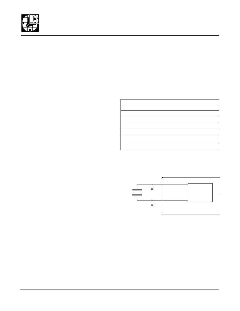
The external crystal will be applied to the XTAL_1 / REF_IN
and XTAL_2 input pins. External crystal load capacitors
are also required.
Recommended External Crystal Configuration
XTAL Load Capacitance Specification = 18 pF
C1
= 27 pF
C2
= 33 pF
External load capacitors C1 and C2 present a load of 15 pf
to the crystal (they are seen in series by the crystal through
the common ground connection). With the additional of PCB
trace capacitance and M908-02 input capacitance, the total
load to the crystal is about 18 pf.
Fvcso
M
Fxtal
×
=
×
M
input crystal frequency
×
Crystal Specifications
Parameter
Min Typ Max Unit
Crystal Type
AT-cut quartz
Mode of Oscillation
Fundamental
f0
Frequency Range
16
40
MHz
ESR
Equivalent Series Resistance
50
Spurious Response (non-harmonic)
-40 dBc
C
L
Load Capacitance,
parallel load resonant
16
32
pF
P0
Drive Level
0.1
1.0
mW
Table 3: Crystal Specifications
XTAL_2
XTAL
XTAL OSC
M9xx-0x
XTAL_1 / REF_IN
C1
C2
M908-02
相關(guān)PDF資料 |
PDF描述 |
|---|---|
| M926-02I600.0000LF | 600 MHz, OTHER CLOCK GENERATOR, CQCC36 |
| M926-02-622.0800LF | 622.08 MHz, OTHER CLOCK GENERATOR, CQCC36 |
| M926-02-622.0800LF | 622.08 MHz, OTHER CLOCK GENERATOR, CQCC36 |
| M926-02I622.0800LF | 622.08 MHz, OTHER CLOCK GENERATOR, CQCC36 |
| M926-02-622.0800 | 622.08 MHz, OTHER CLOCK GENERATOR, CQCC36 |
相關(guān)代理商/技術(shù)參數(shù) |
參數(shù)描述 |
|---|---|
| M9081 | 制造商:Tamura Corporation of America 功能描述: |
| M9088 | 制造商:Motorola Inc 功能描述: |
| M9099 | 制造商:Tamura Corporation of America 功能描述: |
| M90C-1006 | 制造商:Teledyne Relays 功能描述: |
| M90C109095C-08 | 制造商:Harwin 功能描述: |
發(fā)布緊急采購(gòu),3分鐘左右您將得到回復(fù)。