- 您現(xiàn)在的位置:買賣IC網(wǎng) > PDF目錄384643 > M66220FP (Mitsubishi Electric Corporation) 256 x 8-BIT MAIL-BOX PDF資料下載
參數(shù)資料
| 型號: | M66220FP |
| 廠商: | Mitsubishi Electric Corporation |
| 英文描述: | 256 x 8-BIT MAIL-BOX |
| 中文描述: | 256 × 8位企業(yè)郵箱 |
| 文件頁數(shù): | 2/11頁 |
| 文件大小: | 138K |
| 代理商: | M66220FP |
MITSUBISHI
DIGITAL ASSP
M66220SP/FP
256
×
8-BIT MAIL-BOX
2
FUNCTION
The M66220 is a mail box most suitable for inter-MPU data transfer
which is used in a multiport mode. Provision of two pairs of addresses
and data buses in its shared memory cell of 256
×
8 bit configuration
allows independent and asynchronous read/write operations from/to
two access ports of A and B individually.
This allows access to shared memory as simple RAM when viewing
from one MPU. The concurrent accessibility to shared memory from
two MPUs provides remarkable improvement of a multiport mode
processor system in throughput.
The arbitration function incorporated in the chip decides the first-in
port to assign a higher priority to the access from one MPU, even if
two MPUs contend for selection of the same address in shared
memory from ports A and B. A Not Ready signal “L” is output to the
last-in port and invalidates any access from the other MPU.
As a write operation to memory, one of addresses A
0
to A
7
is specified.
The CS signal is set to “L” to place one of I/O pins in the input mode.
Also, the WE signal is set to “L”. Data at the I/O pin is thus written
into memory.
As a read operation, the WE signal is set to “H”. Both CS signal and
OE signal are set to “L” to place one of I/O pins in the output mode.
One of addresses A
0
to A
7
is specified. Data at the specified address
is output to the I/O pin.
When the CS signal is set to “H”, the chip enters a non-select state
which inhibits a read and write operation. At this time, the output is
placed in the floating state (high impedance state), thus allowing OR
tie with another chip. When the OE signal is set to “H”, the output
enters the floating state. In the I/O bus mode, setting the OE signal
to “H” at a write time avoids contention of I/O bus data. When the CS
signal is set to Vcc, the output enters the full stand-by state to minimize
supply current (See Tables 1 and 2).
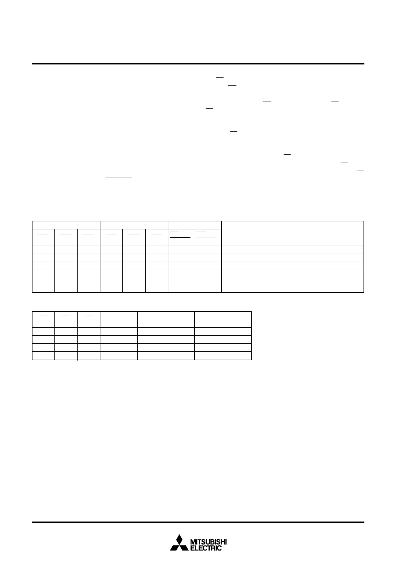
Table 1 Mode Settings of Ports
(A
0
A ~ A
7
A
≠
A
0
B ~ A
7
B)
A port input
B port input
Flag
CSA
H
×
L
L
×
×
WEA
×
×
L
H
×
×
OEA
×
×
×
L
×
×
CSB
×
H
×
×
L
L
WEB
×
×
×
×
L
H
OEB
×
×
×
×
×
L
Not
Ready A
H
H
H
H
H
H
Not
Ready B
H
H
H
H
H
H
Operation
A port is set to the non-select mode.
B port is set to the non-select mode.
A port is set to the write mode for memory.
A port is set to the read mode for memory.
B port is set to the write mode for memory.
B port is set to the read mode for memory.
Table 2 Basic Functions of Ports
CS
H
L
L
L
WE
×
L
H
H
OE
×
×
L
H
Mode
Non-select
Write
Read
I/O pin
High impedance
D
IN
D
OUT
High impedance
I
CC
Stand-by
Operation
Operation
Operation
Note 1:
×
indicates “L” or “H”. (Irrelevant)
“H” = High level, “L” = Low level
相關(guān)PDF資料 |
PDF描述 |
|---|---|
| M66220SP | 256 x 8-BIT MAIL-BOX |
| M66222SP | POT THUMBWHEEL 5K OHM AUDIO |
| M66222FP | 128 x 8-BIT x 2 MAIL-BOX |
| M66255FP | Cable Ties; Pack Quantity:1000 RoHS Compliant: Yes |
| M66273FP | LCD CONTROLLER with VRAM |
相關(guān)代理商/技術(shù)參數(shù) |
參數(shù)描述 |
|---|---|
| M66220SP | 制造商:RENESAS 制造商全稱:Renesas Technology Corp 功能描述:256*8-BIT MAIL-BOX |
| M66221FP | 制造商:MITSUBISHI 制造商全稱:Mitsubishi Electric Semiconductor 功能描述:256 x 9-BIT MAIL-BOX |
| M66221SP | 制造商:MITSUBISHI 制造商全稱:Mitsubishi Electric Semiconductor 功能描述:256 x 9-BIT MAIL-BOX |
| M66222FP | 制造商:MITSUBISHI 制造商全稱:Mitsubishi Electric Semiconductor 功能描述:128 x 8-BIT x 2 MAIL-BOX |
| M66222SP | 制造商:RENESAS 制造商全稱:Renesas Technology Corp 功能描述:128*8-BIT*2 MAIL-BOX |
發(fā)布緊急采購,3分鐘左右您將得到回復(fù)。