- 您現(xiàn)在的位置:買(mǎi)賣(mài)IC網(wǎng) > PDF目錄377830 > M50LPW012K1T (意法半導(dǎo)體) 2 Mbit 256Kb x8, Boot Block 3V Supply Low Pin Count Flash Memory PDF資料下載
參數(shù)資料
| 型號(hào): | M50LPW012K1T |
| 廠商: | 意法半導(dǎo)體 |
| 英文描述: | 2 Mbit 256Kb x8, Boot Block 3V Supply Low Pin Count Flash Memory |
| 中文描述: | 2兆位的256Kb × 8,啟動(dòng)塊3V電源低引腳數(shù)快閃記憶體 |
| 文件頁(yè)數(shù): | 7/35頁(yè) |
| 文件大?。?/td> | 239K |
| 代理商: | M50LPW012K1T |
第1頁(yè)第2頁(yè)第3頁(yè)第4頁(yè)第5頁(yè)第6頁(yè)當(dāng)前第7頁(yè)第8頁(yè)第9頁(yè)第10頁(yè)第11頁(yè)第12頁(yè)第13頁(yè)第14頁(yè)第15頁(yè)第16頁(yè)第17頁(yè)第18頁(yè)第19頁(yè)第20頁(yè)第21頁(yè)第22頁(yè)第23頁(yè)第24頁(yè)第25頁(yè)第26頁(yè)第27頁(yè)第28頁(yè)第29頁(yè)第30頁(yè)第31頁(yè)第32頁(yè)第33頁(yè)第34頁(yè)第35頁(yè)
7/35
M50LPW012
Note that, during a Bus Write operation, the
Command
Interface
command as soon as the data is fully received; a
Bus Abort during the final TAR cycles is not
guaranteed to abort the command; the bus,
however, will be released immediately.
Standby.
When LFRAME is High, V
IH
, the
memory is put into Standby mode where LAD0-
LAD3 are put into a high-impedance state and the
Supply Current is reduced to the Standby level,
I
CC1
.
Reset.
During Reset mode all internal circuits are
switched off, the memory is deselected and the
outputs are put in high-impedance. The memory is
in Reset mode when Interface Reset, RP, or CPU
Reset, INIT, is Low, V
IL
. RP or INIT must be held
Low, V
IL
, for t
PLPH
. The memory resets to Read
mode upon return from Reset mode and the Lock
Registers return to their default states regardless
of their state before Reset, see Table 16. If RP or
INIT goes Low, V
IL
, during a Program or Erase
operation, the operation is aborted and the
memory cells affected no longer contain valid
data; the memory can take up to t
PLRH
to abort a
Program or Erase operation.
Block Protection.
Block
forced using the signals Top Block Lock, TBL, and
Write Protect, WP, regardless of the state of the
Lock Registers.
Address/Address Multiplexed (A/A Mux) Bus
Operations
The Address/Address Multiplexed (A/A Mux)
Interface has a more traditional style interface.
The signals consist of a multiplexed address
signals (A0-A10), data signals, (DQ0-DQ7) and
three control signals (RC, G, W). An additional
signal, RP, can be used to reset the memory.
starts
executing
the
Protection
can
be
The Address/Address Multiplexed (A/A Mux)
Interface
is
included
Programming equipment
programming. Only a subset of the features
available to the Low Pin Count (LPC) Interface are
available; these include all the Commands but
exclude the Security features and other registers.
The following operations can be performed using
the appropriate bus cycles: Bus Read, Bus Write,
Output Disable and Reset.
When the Address/Address Multiplexed (A/A Mux)
Interface is
selected all the blocks
unprotected. It is not possible to protect any blocks
through this interface.
Bus Read.
Bus Read operations are used to
output the contents of the Memory Array, the
Electronic Signature and the Status Register. A
valid Bus Read operation begins by latching the
Row Address and Column Address signals into
the memory using the Address Inputs, A0-A10,
and the Row/Column Address Select RC. Then
Write Enable (W) and Interface Reset (RP) must
be High, V
IH
, and Output Enable, G, Low, V
IL
, in
order to perform a Bus Read operation. The Data
Inputs/Outputs will output the value, see Figure
11, A/A Mux Interface Read AC Waveforms, and
Table 25, A/A Mux Interface Read AC
Characteristics, for details of when the output
becomes valid.
Bus Write.
Bus Write operations write to the
Command Interface. A valid Bus Write operation
begins by latching the Row Address and Column
Address signals into the memory using the
Address Inputs, A0-A10, and the Row/Column
Address Select RC. The data should be set up on
the Data Inputs/Outputs; Output Enable, G, and
Interface Reset, RP, must be High, V
IH
and Write
Enable, W, must be Low, V
IL
. The Data Inputs/
Outputs are latched on the rising edge of Write
Enable, W. See Figure 12, A/A Mux Interface
Write AC Waveforms, and Table 26, A/A Mux
Interface Write AC Characteristics, for details of
the timing requirements.
Output Disable.
The data outputs are high-im-
pedance when the Output Enable, G, is at V
IH
.
Reset.
During Reset mode all internal circuits are
switched off, the memory is deselected and the
outputs are put in high-impedance. The memory is
in Reset mode when RP is Low, V
IL
. RP must be
held Low, V
IL
for t
PLPH
. If RP is goes Low, V
IL
,
during a Program or Erase operation, the
operation is aborted and the memory cells affected
no longer contain valid data; the memory can take
up to t
PLRH
to abort a Program or Erase operation.
for
use
faster factory
by
Flash
for
are
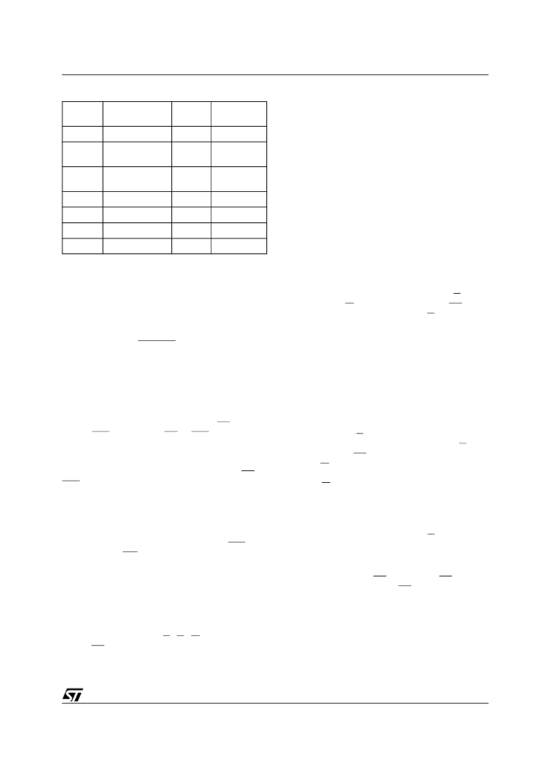
Table 6. Block Addresses
Note: For A19:18 values, refer to Table 2.
Size
(KBytes)
Address Range
Block
Number
Block Type
16
3C000h-3FFFFh
6
Boot Block
8
3A000h-3BFFFh
5
Parameter
Block
8
38000h-39FFFh
4
Parameter
Block
32
30000h-37FFFh
3
Main Block
64
20000h-2FFFFh
2
Main Block
64
10000h-1FFFFh
1
Main Block
64
00000h-0FFFFh
0
Main Block
相關(guān)PDF資料 |
PDF描述 |
|---|---|
| M50LPW040 | 4 Mbit 512Kb x8, Uniform Block 3V Supply Low Pin Count Flash Memory |
| M50LPW040K | 4 Mbit 512Kb x8, Uniform Block 3V Supply Low Pin Count Flash Memory |
| M50LPW040K1T | 4 Mbit 512Kb x8, Uniform Block 3V Supply Low Pin Count Flash Memory |
| M50LPW040K5T | 4 Mbit 512Kb x8, Uniform Block 3V Supply Low Pin Count Flash Memory |
| M50LPW040N | 4 Mbit 512Kb x8, Uniform Block 3V Supply Low Pin Count Flash Memory |
相關(guān)代理商/技術(shù)參數(shù) |
參數(shù)描述 |
|---|---|
| M50LPW040 | 制造商:STMICROELECTRONICS 制造商全稱:STMicroelectronics 功能描述:4 Mbit 512Kb x8, Uniform Block 3V Supply Low Pin Count Flash Memory |
| M50LPW040K | 制造商:STMICROELECTRONICS 制造商全稱:STMicroelectronics 功能描述:4 Mbit 512Kb x8, Uniform Block 3V Supply Low Pin Count Flash Memory |
| M50LPW040K1 | 功能描述:閃存 3.6V 4M (512Kx8) RoHS:否 制造商:ON Semiconductor 數(shù)據(jù)總線寬度:1 bit 存儲(chǔ)類型:Flash 存儲(chǔ)容量:2 MB 結(jié)構(gòu):256 K x 8 定時(shí)類型: 接口類型:SPI 訪問(wèn)時(shí)間: 電源電壓-最大:3.6 V 電源電壓-最小:2.3 V 最大工作電流:15 mA 工作溫度:- 40 C to + 85 C 安裝風(fēng)格:SMD/SMT 封裝 / 箱體: 封裝:Reel |
| M50LPW040K1T | 制造商:STMICROELECTRONICS 制造商全稱:STMicroelectronics 功能描述:4 Mbit 512Kb x8, Uniform Block 3V Supply Low Pin Count Flash Memory |
| M50LPW040K5T | 制造商:STMICROELECTRONICS 制造商全稱:STMicroelectronics 功能描述:4 Mbit 512Kb x8, Uniform Block 3V Supply Low Pin Count Flash Memory |
發(fā)布緊急采購(gòu),3分鐘左右您將得到回復(fù)。