- 您現(xiàn)在的位置:買賣IC網(wǎng) > PDF目錄45050 > M48ST59W-70MH1TR (STMICROELECTRONICS) 0 TIMER(S), REAL TIME CLOCK, PDSO44 PDF資料下載
參數(shù)資料
| 型號(hào): | M48ST59W-70MH1TR |
| 廠商: | STMICROELECTRONICS |
| 元件分類: | 時(shí)鐘/數(shù)據(jù)恢復(fù)及定時(shí)提取 |
| 英文描述: | 0 TIMER(S), REAL TIME CLOCK, PDSO44 |
| 封裝: | 0.330 INCH, SNAPHAT, PLASTIC, SOH-44 |
| 文件頁數(shù): | 14/29頁 |
| 文件大?。?/td> | 158K |
| 代理商: | M48ST59W-70MH1TR |
第1頁第2頁第3頁第4頁第5頁第6頁第7頁第8頁第9頁第10頁第11頁第12頁第13頁當(dāng)前第14頁第15頁第16頁第17頁第18頁第19頁第20頁第21頁第22頁第23頁第24頁第25頁第26頁第27頁第28頁第29頁

21/29
M48ST59W
Power-Fail Comparator
The Power-Fail Input (PFI) is compared to an in-
ternal reference voltage (independent from the
VPFD comparator). If PFI is less than the power-fail
threshold (VPFI), the Power-Fail Output (PFO) will
go low. This function is intended for use as an un-
dervoltage detector to signal a failing power sup-
ply. Typically PFI is connected through an external
voltage divider to either the unregulated DC input
(if it is available) or the regulated output of the VCC
regulator. The voltage divider can be set up such
that the voltage at PFI falls below VPFI several mil-
liseconds before the regulated VCC input to the
M48ST59W or the microprocessor drops below
the minimum operating voltage.
During battery back-up, the power-fail comparator
turns off and PFO goes (or remains) low. This oc-
curs after VCC drops below VPFD(min). When pow-
er returns, PFO is forced high, irrespective of VPFI
for the write protect time (tREC), which is the time
from VPFD (max) until the inputs are recognized. At
the end of this time, the power-fail comparator is
enabled and PFO follows PFI. If the comparator is
unused, PFI should be connected to VSS and PFO
left unconnected.
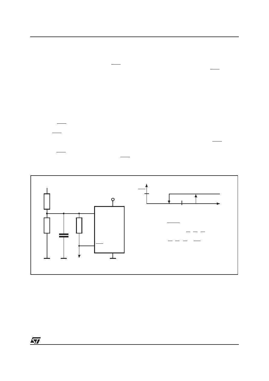
Hysteresis may be added to PFI for additional
noise margin if desired (see Figure 12). The ratio
of R1 and R2 should be selected such that PFI
sees VPFI when VIN falls to its trip point (VTRIP).
Connecting R3 between PFI and PFO provides
the hysteresis and should typically be more than
ten (10) times the value of R1 or R2. The hystere-
sis window will extend both above (VH) and below
(VL) the original trip point (Vt). Connecting an ordi-
nary signal diode in series with R3 causes the low-
er trip point (VL) to coincide with the trip point
without hysteresis, so the entire hysteresis window
occurs above VTRIP (see Figure 13, page 22). This
method provides additional noise margin without
compromising the accuracy of the power-fail
threshold when the monitored voltage is falling.
The current through R1 and R2 should be at least
1uA to ensure that the 25nA PFI input current does
not shift the trip point. R3 should be larger than
82K Ohms to avoid loading down the PFO pin. The
capacitor C1 is added for noise rejection, but is op-
tional.
Figure 12. Adding Hysteresis
PFO
VCC
PFI
R3
R2
R1
VIN
C1
GND
TO
CONTROLLER
VIN
0V
PFO
VL
VH
VTRIP
VTRIP =VPFI
R1 + R2
R2
VH =
1+ 1+ 1
R1
VPFI + VPFH
()
R1
()
R2
R3
VL =R1
()
1+ 1 + 1
R1
VPFI
R2
R3
VCC
R3
–
where
VPFH = 10mV
VPFI = 1.25V
[]
()
AI04611
相關(guān)PDF資料 |
PDF描述 |
|---|---|
| M48ST59W-100MH1 | 0 TIMER(S), REAL TIME CLOCK, PDSO44 |
| M48T02-150PC1 | 0 TIMER(S), REAL TIME CLOCK, PDIP24 |
| M48T18-100MH1TR | 0 TIMER(S), REAL TIME CLOCK, PDSO28 |
| M48T18-100MH1 | 0 TIMER(S), REAL TIME CLOCK, PDSO28 |
| M48T18-150PC1 | 0 TIMER(S), REAL TIME CLOCK, PDIP28 |
相關(guān)代理商/技術(shù)參數(shù) |
參數(shù)描述 |
|---|---|
| M48T02 | 制造商:STMICROELECTRONICS 制造商全稱:STMicroelectronics 功能描述:5.0V, 16 Kbit (2Kb x 8) TIMEKEEPER SRAM |
| M48T02_03 | 制造商:STMICROELECTRONICS 制造商全稱:STMicroelectronics 功能描述:5.0V, 16 Kbit (2Kb x 8) TIMEKEEPER㈢ SRAM |
| M48T02_07 | 制造商:STMICROELECTRONICS 制造商全稱:STMicroelectronics 功能描述:5.0V, 16 Kbit (2Kb x 8) TIMEKEEPER SRAM |
| M48T02_10 | 制造商:STMICROELECTRONICS 制造商全稱:STMicroelectronics 功能描述:5.0 V, 16 Kbit (2 Kb x 8) TIMEKEEPER? SRAM |
| M48T02-120PC1 | 制造商:STMICROELECTRONICS 制造商全稱:STMicroelectronics 功能描述:CMOS 8K x 8 TIMEKEEPER SRAM |
發(fā)布緊急采購,3分鐘左右您將得到回復(fù)。