- 您現(xiàn)在的位置:買賣IC網(wǎng) > PDF目錄299434 > M470T2953CZ3-CE7 128M X 64 DDR DRAM MODULE, 0.4 ns, ZMA200 PDF資料下載
參數(shù)資料
| 型號: | M470T2953CZ3-CE7 |
| 元件分類: | DRAM |
| 英文描述: | 128M X 64 DDR DRAM MODULE, 0.4 ns, ZMA200 |
| 封裝: | ROHS COMPLIANT, SODIMM-200 |
| 文件頁數(shù): | 15/20頁 |
| 文件大小: | 355K |
| 代理商: | M470T2953CZ3-CE7 |
Rev. 1.6 March 2007
SODIMM
DDR2 SDRAM
Page 4 of 20
Note :
1. “Z” of Part number(11th digit) stand for Lead-free products.
2. “3” of Part number(12th digit) stand for Dummy Pad PCB products.
Part Number
Density
Organization
Component Composition
Number of Rank
Height
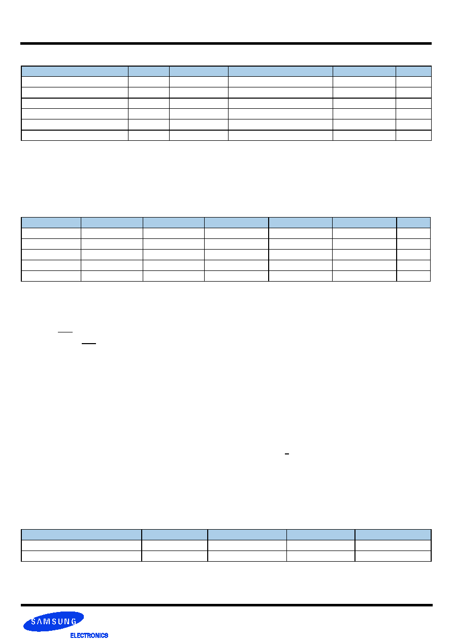
M470T3354CZ3-C(L)E7/F7/E6/D5/CC
256MB
32Mx64
32Mx16(K4T51163QC)*4
1
30mm
M470T3354CZ0-C(L)E7/F7/E6/D5/CC
256MB
32Mx64
32Mx16(K4T51163QC)*4
1
30mm
M470T6554CZ3-C(L)E7/F7/E6/D5/CC
512MB
64Mx64
32Mx16(K4T51163QC)*8
2
30mm
M470T6554CZ0-C(L)E7/F7/E6/D5/CC
512MB
64Mx64
32Mx16(K4T51163QC)*8
2
30mm
M470T2953CZ3-C(L)E7/F7/E6/D5/CC
1GB
128Mx64
64Mx8(K4T51083QC)*16
2
30mm
M470T2953CZ0-C(L)E7/F7/E6/D5/CC
1GB
128Mx64
64Mx8(K4T51083QC)*16
2
30mm
Performance range
JEDEC standard 1.8V ± 0.1V Power Supply
VDDQ = 1.8V ± 0.1V
200 MHz fCK for 400Mb/sec/pin, 267MHz fCK for 533Mb/sec/pin, 333MHz fCK for 667Mb/sec/pin, 400MHz fCK for 800Mb/sec/pin
4 Banks
Posted CAS
Programmable CAS Latency: 3, 4, 5, 6
Programmable Additive Latency: 0, 1 , 2 , 3 , 4 , 5
Write Latency(WL) = Read Latency(RL) -1
Burst Length: 4 , 8(Interleave/nibble sequential)
Programmable Sequential / Interleave Burst Mode
Bi-directional Differential Data-Strobe (Single-ended data-strobe is an optional feature)
Off-Chip Driver(OCD) Impedance Adjustment
On Die Termination with selectable values(50/75/150 ohms or disable)
PASR(Partial Array Self Refresh)
Average Refresh Period 7.8us at lower than a TCASE 85°C, 3.9us at 85°C < TCASE < 95 °C
- support High Temperature Self-Refresh rate enable feature
Package: 60ball FBGA - 64Mx8 , 84ball FBGA - 32Mx16
All of Lead-free products are compliant for RoHS
E7 (DDR2-800)
F7 (DDR2-800)
E6 (DDR2-667)
D5 (DDR2-533)
CC (DDR2-400)
Unit
Speed@CL3
400
-
400
Mbps
Speed@CL4
533
400
Mbps
Speed@CL5
800
667
533
-
Mbps
Speed@CL6
-
800
-
Mbps
CL-tRCD-tRP
5-5-5
6-6-6
5-5-5
4-4-4
3-3-3
CK
Organization
Row Address
Column Address
Bank Address
Auto Precharge
64Mx8(512Mb) based Module
A0-A13
A0-A9
BA0-BA1
A10
32Mx16(512Mb) based Module
A0-A12
A0-A9
BA0-BA1
A10
1.0 DDR2 Unbuffered SODIMM Ordering Information
2.0 Features
3.0 Address Configuration
相關(guān)PDF資料 |
PDF描述 |
|---|---|
| M485L1624FT0-LA2 | 16M X 72 DDR DRAM MODULE, 0.75 ns, DMA200 |
| M485L1624FT0-CB3 | 16M X 72 DDR DRAM MODULE, 0.7 ns, DMA200 |
| M5-NP | UNSHIELDED, 0.056 uH - 0.12 uH, VARIABLE INDUCTOR, SMD |
| M504-7885022 | 50 CONTACT(S), MALE, RIGHT ANGLE PCMCIA CONNECTOR, SURFACE MOUNT |
| M50FLW080AN5G | 1M X 8 FLASH 3V PROM, 11 ns, PDSO40 |
相關(guān)代理商/技術(shù)參數(shù) |
參數(shù)描述 |
|---|---|
| M470T2953CZ3-CLCC | 制造商:SAMSUNG 制造商全稱:Samsung semiconductor 功能描述:DDR2 Unbuffered SODIMM 200pin Unbuffered SODIMM based on 512Mb C-die 64bit Non-ECC |
| M470T2953CZ3-CLD5 | 制造商:SAMSUNG 制造商全稱:Samsung semiconductor 功能描述:DDR2 Unbuffered SODIMM 200pin Unbuffered SODIMM based on 512Mb C-die 64bit Non-ECC |
| M470T2953CZ3-CLE6 | 制造商:SAMSUNG 制造商全稱:Samsung semiconductor 功能描述:DDR2 Unbuffered SODIMM 200pin Unbuffered SODIMM based on 512Mb C-die 64bit Non-ECC |
| M470T2953CZ3-CLE7 | 制造商:SAMSUNG 制造商全稱:Samsung semiconductor 功能描述:DDR2 Unbuffered SODIMM 200pin Unbuffered SODIMM based on 512Mb C-die 64bit Non-ECC |
| M470T2953EZ3CE600 | 制造商:Samsung Semiconductor 功能描述: |
發(fā)布緊急采購,3分鐘左右您將得到回復(fù)。