- 您現(xiàn)在的位置:買賣IC網(wǎng) > PDF目錄359061 > M41T256YMT (意法半導(dǎo)體) 256 Kbit 32K x8 SERIAL RTC PDF資料下載
參數(shù)資料
| 型號(hào): | M41T256YMT |
| 廠商: | 意法半導(dǎo)體 |
| 英文描述: | 256 Kbit 32K x8 SERIAL RTC |
| 中文描述: | 256千位32K的x8串行實(shí)時(shí)時(shí)鐘 |
| 文件頁(yè)數(shù): | 12/26頁(yè) |
| 文件大?。?/td> | 363K |
| 代理商: | M41T256YMT |
第1頁(yè)第2頁(yè)第3頁(yè)第4頁(yè)第5頁(yè)第6頁(yè)第7頁(yè)第8頁(yè)第9頁(yè)第10頁(yè)第11頁(yè)當(dāng)前第12頁(yè)第13頁(yè)第14頁(yè)第15頁(yè)第16頁(yè)第17頁(yè)第18頁(yè)第19頁(yè)第20頁(yè)第21頁(yè)第22頁(yè)第23頁(yè)第24頁(yè)第25頁(yè)第26頁(yè)
M41T256Y
12/26
READ Mode
In this mode the master reads the M41T256Y
slave after setting the slave address (see Figure
11, page 12). Following the WRITE Mode Control
Bit (R/W=0) and the Acknowledge Bit, the byte ad-
dresses A(0) and A(1) are written to the on-chip
address pointer (MSB of address byte A(0) is a
“Don’t care”). Next the START condition and slave
address are repeated followed by the READ Mode
Control Bit (R/W=1). At this point the master trans-
mitter becomes the master receiver. The data byte
which was addressed will be transmitted and the
master receiver will send an acknowledge bit to
the slave transmitter. The address pointer is only
incremented on reception of an Acknowledge
Clock. The M41T256Y slave transmitter will now
place the data byte at address An+1 on the bus,
the master receiver reads and acknowledges the
new byte and the address pointer is incremented
to An+2.
This cycle of reading consecutive addresses will
continue until the master receiver sends a STOP
condition to the slave transmitter (see Figure 12,
page 13).
Note:
Address pointer will wrap around from max-
imum address to minimum address if consecutive
READ or WRITE cycles are performed.
An alternate READ Mode may also be implement-
ed whereby the master reads the M41T256Y slave
without first writing to the (volatile) address point-
er. The first address that is read is the last one
stored in the pointer (see Figure 13, page 13).
WRITE Mode
In this mode the master transmitter transmits to
the M41T256Y slave receiver. Bus protocol is
shown in Figure Figure 14, page 13. Following the
START condition and slave address, a logic '0' (R/
W=0) is placed on the bus and indicates to the ad-
dressed device that byte addresses A(0) and A(1)
will follow and is to be written to the on-chip ad-
dress pointer (MSB of address byte A(0) is a
“Don’t care”). The data byte to be written to the
memory is strobed in next and the internal address
pointer is incremented to the next memory location
within the RAM on the reception of an acknowl-
edge bit. The M41T256Y slave receiver will send
an acknowledge bit to the master transmitter after
it has received the slave address (see Figure 11,
page 12) and again after it has received each ad-
dress byte.
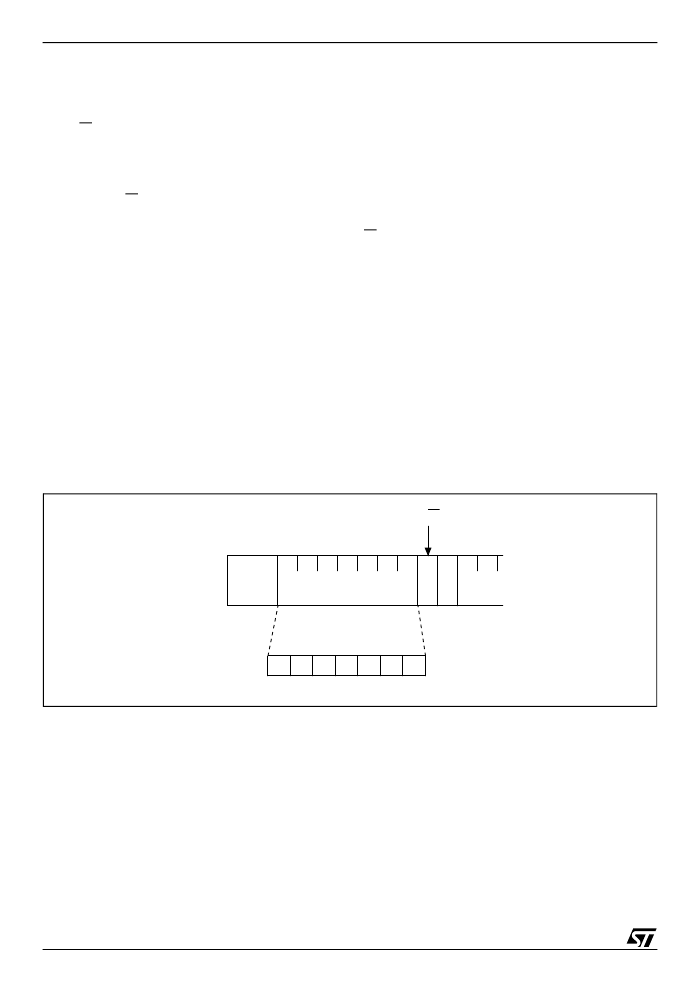
Figure 11. Slave Address Location
Note: The most significant bit is sent first.
AI00602
R/W
SLAVE ADDRESS
START
A
0
1
0
0
0
1
1
M
L
相關(guān)PDF資料 |
PDF描述 |
|---|---|
| M41T256YMT7TR | RCA-F TO RCA-F COUPLER |
| M41T256YMT7 | RCA F TO BNC-M ADAPTER |
| M41T315W-65MH6E | Serial Access Phantom RTC Supervisor |
| M41T315W-65MH6F | Serial Access Phantom RTC Supervisor |
| M41T315W-65MH6TR | Serial Access Phantom RTC Supervisor |
相關(guān)代理商/技術(shù)參數(shù) |
參數(shù)描述 |
|---|---|
| M41T256YMT7 | 功能描述:實(shí)時(shí)時(shí)鐘 Serial 256K (32Kx8) RoHS:否 制造商:Microchip Technology 功能:Clock, Calendar. Alarm RTC 總線接口:I2C 日期格式:DW:DM:M:Y 時(shí)間格式:HH:MM:SS RTC 存儲(chǔ)容量:64 B 電源電壓-最大:5.5 V 電源電壓-最小:1.8 V 最大工作溫度:+ 85 C 最小工作溫度: 安裝風(fēng)格:Through Hole 封裝 / 箱體:PDIP-8 封裝:Tube |
| M41T256YMT7E | 功能描述:實(shí)時(shí)時(shí)鐘 Serial 256K (32Kx8) RoHS:否 制造商:Microchip Technology 功能:Clock, Calendar. Alarm RTC 總線接口:I2C 日期格式:DW:DM:M:Y 時(shí)間格式:HH:MM:SS RTC 存儲(chǔ)容量:64 B 電源電壓-最大:5.5 V 電源電壓-最小:1.8 V 最大工作溫度:+ 85 C 最小工作溫度: 安裝風(fēng)格:Through Hole 封裝 / 箱體:PDIP-8 封裝:Tube |
| M41T256YMT7F | 功能描述:實(shí)時(shí)時(shí)鐘 Serial 256K (32Kx8) RoHS:否 制造商:Microchip Technology 功能:Clock, Calendar. Alarm RTC 總線接口:I2C 日期格式:DW:DM:M:Y 時(shí)間格式:HH:MM:SS RTC 存儲(chǔ)容量:64 B 電源電壓-最大:5.5 V 電源電壓-最小:1.8 V 最大工作溫度:+ 85 C 最小工作溫度: 安裝風(fēng)格:Through Hole 封裝 / 箱體:PDIP-8 封裝:Tube |
| M41T256YMT7TR | 制造商:STMICROELECTRONICS 制造商全稱:STMicroelectronics 功能描述:256 Kbit 32K x8 SERIAL RTC |
| M41T256YSH | 制造商:STMICROELECTRONICS 制造商全稱:STMicroelectronics 功能描述:256 Kbit 32K x8 SERIAL RTC |
發(fā)布緊急采購(gòu),3分鐘左右您將得到回復(fù)。